1. Electrical Foundations
Digital circuits are a special class of electrical circuits that operate with discrete values of voltages. In today’s digital systems, we use two voltages to represent discrete values, high and low voltage. The specific voltage values are of secondary importance, and vary across different implementations and technologies. Of course, most of us have experienced voltage as a phenomenon of the macroscopic, continuous world, where switching between high and low voltages is not an instantaneous event but a continuous process that takes time to transition through intermediate voltages. If the time to switch between voltages is irrelevant compared to the time the system rests at a particular voltage, we may consider the two relevant states of high and low voltage only, and disregard the intermediate voltages during the transition. This focus on the essential property of interest, the steady voltages rather than the transition between them, is part of the digital abstraction.
The digital abstraction is the basis of digital logic. An important application of digital logic is to argue about the correctness of programs, where we care about sequences of discrete states. To keep such arguments comprehensible, we ignore the details of how the transition between states occurs at the voltage level. However, the speed of the transition is the crucial property that determines the performance of a computation. Since electrical processes are blazingly fast, and can be controlled in a highly reliable and reproducible fashion, we build today’s computers with electrical circuits, digital circuits to be precise. Speed is an important property of digital circuits, not only because faster circuits enable faster computers, but also because faster circuits consume more power than slow circuits. For example, when targeting low-power computers for cell phones, we may trade speed for reduced power consumption. Thus, knowing how to design fast versus slow digital circuits is essential for computer engineers, just like the techniques to build a Porsche differ from those for a Trabi. This chapter recaps the electrical foundations of digital circuits, as far as we need them to understand both their logical functionality and speed.
1.1. Current, Voltage, and Energy
We begin with a review of the basic concepts that enable us to understand the phenomena associated with electricity: charge, current, voltage, energy, and power.
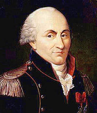
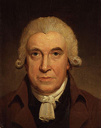
(1736-1806)
Electrical charge is a fundamental property of matter. Regular mortals can neither create nor destroy electrical charge. Consequently, in our circuits charge is conserved by nature. An electron has the smallest unit of charge that exists, the negated elementary charge
and a positron has a positive elementary charge \(q.\)
Unit \(C\) honors the French physicist Coulomb, who formulated the law that describes the electrostatic force between two charges \(q_1\) and \(q_2\)
where constant \(k = 8.99 \times 10^9\,N m^2 / C^2\) and \(d\) is the distance between the charges. Force \(F\) is attractive, if the charges have opposite signs, otherwise \(F\) is repulsive. We can imagine the force as a vector field. In free space, the field emanates radially from an electrical charge. The direction of the field gives the direction of the force on a positive test charge. In Figure 1.1, the field lines of an electron point toward the electron, indicating that the electron attracts a positive test charge, whereas the field lines of the positron point outwards, because a positron repells a positive test charge.

Figure 1.1: Negative and positive electrical charges and their fields.
An electron experiences the force field of a charge at distance \(d=1 mm\) (milli-meter). The force of \(F = 9.81 mN\) (milli-Newton) attracts the electron. This is the force mother Earth’s gravity exerts on a mass weighing \(1 g\) (gram). How big and of which type is the charge?
Answer: The charge must be positive, because it attracts the electron. If the electron has charge \(q_1 = -1.602 \times 10^{-19} C,\) the charge at distance \(d\) is
which is the charge of approximately \(4.25 \times 10^{19} (\approx q_2 / q)\) positrons. In this calculation, we presume that an attractive force is negative, so that the minus signs of the force and electron charge cancel each other out, and \(q_2\) is positive.
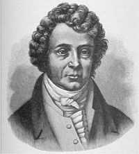
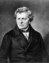
(1775–1836)
An electrical current is charge in motion. Quantitatively, current \(i\) is a rate, the number of charges moved through an area per unit of time. The area may be the cross section of a wire, for example. In general, current \(i(t) = dq / dt\) changes instantaneously over time \(t,\) i.e. the current is the derivative of \(q\) with respect to \(t.\) We refer to the average current \(I = \Delta q / \Delta t\) over finite time period \(\Delta t\) with an upper case letter \(I.\) The unit for current is the Ampere, \(1 A = 1 C/s,\) in honor of the French physicist Ampère.
A cell phone battery is rated to produce \(1 A h\) (amp \(\cdot\) hour). How long does the battery last if the phone draws an average current of \(100 mA\)?
Answer: Battery ratings state the capacity or, more precisely, the total charge \(Q\) the battery can produce. Rather than using Coulombs, battery manufacturers prefer the unit amp-hour. Since one hour has 3600 seconds, \(1 A h = 3600 A s = 3600 C.\) If we discharge the battery at a rate of \(1 A,\) i.e. we consume current \(I = 1 A\) on average, the battery lasts for one hour. If the average current is only \(I = 100 mA,\) we can draw this current for a longer time period of time:
This straightforward calculation surely confirms your intuition: your phone will last longer if you talk less or plug in a battery with larger capacity.
Electrical charges flow through wires pretty much like water flows through pipes. Therefore, we sometimes use fluids as an aid for imagining how electrical currents flow through circuits, including practically useful circuits with producer and consumer devices. Figure 1.2 contrasts circuits built from pipes and wires.

Figure 1.2: On the left, a fluid flow is produced by a pump and energy is consumed by a turbine. On the right, an electrical current is produced by a battery and energy is consumed by a light bulb.
Consider the closed water loop on the left of Figure 1.2 that connects a pump and a turbine. The pump generates a flow of water, which is used to rotate the turbine. In such a system, the flow \(U\) of water atoms per time unit is the same everywhere in the loop, and in particular before and after the turbine. However, the water pressure \(P_H\) before the turbine is higher than water pressure \(P_L\) after the turbine. The pressure difference represents the energy that the turbine transforms into rotations. The analogon to the water loop is the electrical circuit shown on the right in Figure 1.2. The battery generates an electrical current that causes the bulb to light up. The current \(I\) is the same before and after the light bulb. Analogous to the water pressure, voltage \(V_H\) before the light bulb is higher than voltage \(V_L\) after the bulb. The voltage difference represents the energy that the light bulb transforms into light and heat.
(1818-1889)
Electrical energy represents the effort required to move an electrical charge through an electrical field, for example inside a wire or a device. We use symbol \(w\) to denote energy, and the unit Joule (\(J\)) in honor of the English physicist Joule.
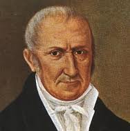
(1745-1827)
Voltage measures the energy (in Joule) to move a positive unit of charge (1 Coulomb) against the force of an electrical field. We use symbol \(v\) for voltage, and unit Volt, \(1 V = 1 J / C,\) in honor of the Italian physicist Volta. Formally, voltage is defined as the derivative \(v = d w / d q.\) Constant or average voltage is denoted with upper case \(V.\)[1]
The voltage difference across the light bulb in Figure 1.2 is \(V = V_H - V_L.\) This is the voltage the battery exerts on the bulb. If the light bulb transforms \(100 J\) of electrical energy in \(1 s\) into light and heat, and the battery generates voltage \(V = 230 V,\) what is the current through the circuit and how much charge does the battery move through the bulb in \(1 h\)?
Answer: At a voltage of \(230 V\) the lightbulb requires
of charge to move through within \(1 s.\) Thus, the current through the circuit is \(I = \Delta q/\Delta t = 435 mA.\) To provide light for \(T = 1 h = 3600 s,\) the battery has to supply a total charge of \(Q = I \cdot T = 435 mA h,\) or in Coulomb \(Q = 0.435 A \cdot 3600 s = 1565.2 C.\)
(1736-1819)
Electrical power is the rate at which electrical energy is consumed per time unit (or produced by a power source):
We use the symbol \(p\) for power, and the unit Watt, \(1 W = 1 J / s = 1 V A,\) in honor of the Scottish engineer Watt. The average power \(P = \Delta w/\Delta t = V \cdot I\) is the average energy consumed per unit of time.
Electrical appliances like microwave ovens or light bulbs are commonly characterized by their power consumption, e.g. a \(10 W\) light bulb or a \(900 W\) microwave. In contrast, the monthly electricity bill for your household is commonly based on the price for energy, e.g. 8 Cent per \(kWh\) (kilo-Watt-hour). How much do you need to pay for electricity if you use the microwave for \(2 h\) and the light bulb for \(150 h\)?
Answer: Power denotes the energy consumption per time unit. The total energy consumed is determined by the duration for which we use an appliance. Thus, energy is the quantity it’s worth paying for, not power. If the microwave consumes a power of \(900 W,\) then using the microwave for 2 hours consumes an energy of \(900 W \cdot 2 h = 1.8 kWh,\) or in Joule \(900 W \cdot 7200 s = 6480 kJ,\) because \(1 J = 1 W s.\) Analogously, your energy consumption for lighting is \(10 W \cdot 150 h = 1.5 kWh.\) Thus, the monthly electricity bill costs you \((1.8 + 1.5) kWh \cdot 8\) Cent\(/ kWh = 26.4\) Cent.
Determine the electrostatic force between an electron and a proton in a hydrogen atom, assuming that a proton carries a positive elementary charge and the distance between the particles is \(0.53 \times 10^{-10} m.\) What is the mass of a body on the surface of the Earth that experiences the equivalent gravitational force, assuming that the mass of planet Earth is \(5.976 \times 10^{24} kg\) and its radius is \(6378 km\)?
An electron carries a negative elementary charge \(q_e = - 1.602 \times 10^{-19} C\) and the proton positive elementary charge \(q_p = 1.602 \times 10^{-19} C.\) At the given distance of \(d = 0.53 \times 10^{-10} m\) within the hydrogen atom, the electrostatic force between the particles is:
The minus sign indicates that the electrostatic force attracts the particles toward each other.
Newton’s law of gravitation states that the attractive gravitational force between two masses \(m_1\) and \(m_2\) and their centers of mass separated by distance \(r\) is:
where \(G = 6.67 \times 10^{-11} m^3/ (kg\,s^2)\) is the gravitational constant. To determine the mass of a body \(m_b\) on the surface of planet Earth such that the gravitational force equals the electrostatic force within a hydrogen atom, we equate the absolute value of \(F_e\) and \(F_g,\) and solve for \(m_b\):
Given that an electron has a mass of \(9.11 \times 10^{-31} kg,\) body mass \(m_b\) is huge and the mass of planet Earth is humongous. Even though \(r_{Earth} \gg d,\) this comparison indicates that the electrostatic force is significantly stronger than the gravitational force.
If you need a replacement for your rechargeable cell phone battery, you find that battery manufacturers advertise the capacity of their products with different specifications. Show that the rating for a Lithium-Ion battery of \(10.78 Wh\) at \(3.85 V\) is equivalent to the rating of \(2800 mAh.\)
The rating of \(2800 mAh\) specifies an electrical charge, because the unit mAh indicates a product of current and time. Since \(1 mAh = 0.001 A \times 3600 s = 3.6 C,\) the rating tells us that the Lithium-Ion battery is capable of storing a charge of \(3.6 C.\)
In contrast, the rating of \(10.78 Wh\) at \(3.85 V\) specifies the amount of energy that the battery can store. The unit \(Wh\) indicates the product of power and time. Since \(1 Wh = 3600 Ws = 3.6 kJ,\) the rating \(10.78 Wh\) specifies an energy of \(10.78 \times 3.6 kJ = 38.8 kJ.\) The additional information that the battery has a voltage of \(3.85 V\) enables us to deduce the charge it can store. To that end we use the units as a guide, and notice that a charge of \(1 C = 1 A s = 1 Ws / V\) because \(1 W = 1 V A.\) Thus, we find that charge \(Q\) in Coulomb is equal to energy \(E\) in Joule, \(1 J = 1 Ws,\) divided by voltage \(V\) in Volt \(V\):
Since the battery rating specifies energy \(E\) in \(Wh\) and charge \(Q\) in \(mAh,\) we introduce a conversion factor of 1000 to compensate for the milli-prefix of the amps:
Using this formula, we can verify that the battery rating \(Q = 2800 mAh\) is indeed equivalent to the rating \(E = 10.78 Wh\) at \(V = 3.85 V,\) because \(1000 \times (10.78 / 3.85) = 2800.\) The latter rating provides you with the important information that your replacement battery must supply a voltage of \(3.85 V,\) though.
Tesla’s Model S electric car is rated to cover 306 miles at a constant speed of \(55 mph\) (miles-per-hour). The battery pack is capable of storing \(85 kWh,\) and consists of 7104 small Lithium-Ion cells organized in groups of 74 cells connected in parallel and 96 groups connected in series. Assuming that each cell generates \(3.8 V,\) determine the current the battery pack supplies to the electric motor when exhausting the advertised range of 306 miles at a speed of \(55 mph\) and the electrical charge stored in each cell.
The time it takes to cover a range of 306 miles at a constant speed of \(55 mph\) is:
The power consumption during this trip is the average energy supplied by the battery pack over time period \(T\):
The electrical current supplied by the battery pack to the electrical motor of the vehicle is \(I = P / V.\) To determine the voltage of the battery pack, we need to examine the organization of the Lithium-Ion cells within the pack. We note that composing battery cells in series enables us to increase the total voltage whereas composing cells in parallel increases the total current the composition can supply, illustrated in the Figure below. Furthermore, the total energy stored in a composition is the sum of the energies stored in each cell, independent of whether the cells are composed in series or in parallel.

Figure [Series and Parallel Battery Compositions]: On the left, two battery cells are composed in series by connecting the positive terminal of one cell with the negative terminal of the other cell. The total voltage of the composition is the sum of the cell voltages. On the right, two battery cells are composed in parallel by connecting the positive terminals and the negative terminals, respectively. The total voltage of the composition equals that of each cell, but the composition can supply twice the current as a single cell.
Each group of Tesla’s battery pack consists of 74 cells composed in parallel. The total voltage of a group is hence equal to the voltage of a single cell given as \(V_{cell} = 3.8 V.\) The pack is a series composition of 96 groups with a total voltage of
We conclude that the current supplied by the battery pack for \(5.56 h\) driving at a speed of \(55 mph\) is
The total energy of the battery pack is given as \(E_{pack} = 85 kWh.\) Since the total energy is the sum of the energy stored in each of the 7104 cells, the energy capacity of a cell is
This is the energy of a battery cell at voltage \(V_{cell} = 3.8 V.\) Therefore, the electrical charge stored in each cell must be according to Exercise 1.2
Rechargeable Lithium-Ion cells with this capacity are among the most commonly used today. They do not only power electric vehicals but also cell phones, laptops, and many other electronic devices.
1.2. Ohm’s Law
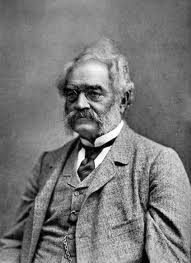
(1789-1854)
A resistor is an electrical device with resistance \(R.\) The unit of resistance is the Ohm, abbreviated with a Greek Omega, \(1 \Omega = 1 V / A,\) in honor of the German physicist Ohm.

Figure 1.3: On the left, fluid flow \(U\) is determined by the smallest cross section of the pipe. On the right, electrical current \(I\) is determined by the resistor.
Figure 1.3 illustrates the analogon between fluid flow through a pipe and electrical current through a wire with a resistor. By conservation of water in a pipe, the same amount of water must flow per time unit through any cross section of the pipe. Therefore, we can restrict the total flow by reducing the cross section at one point in the pipe. Analogously, we can reduce the current flowing through a wire by inserting a resistor.
Ohm discovered that the voltage across a resistor is proportional to the current flowing through it, and identified the resistance as the proportionality constant. This linear relationship between voltage and current is known today as Ohm’s law, and is the reason why unit \(\Omega\) is defined as \(1 \Omega = 1 V / A.\)
Ohm’s law
The voltage across a resistor is proportional to the current flowing through it:
Use upper-case letters to indicate time independent currents and voltages: \(V = R \cdot I.\)
Ohm’s law looks simpler than it is. Recall that voltage forces charges to move in a particular direction, and we have positive and negative charges, that we represent as positive and negative quantities. Ohm’s law assumes conventions about the direction of the voltage and current of the resistor to be applied as intended. The first convention is the sign convention for currents flowing through a wire or two-terminal device like a resistor. A current in the direction of positive charges shall be a positive current. In Figure 1.4, the arrow head indicates that current \(i\) flows top to bottom, i.e. positive charges flow downward. However, most technologies today move electrons, i.e. negative charges, through circuits rather than positive charges. We can produce a positive current either with positive charges moving in the indicated direction, or with negative charges flowing in the opposite direction, or both. Ohm’s law applies to any current, independent of the underlying physical mechanism.

Figure 1.4: Resistor with reference directions for current and voltage.
The second convention involves the use of reference directions for voltages and currents in circuits. We use arrows to specify a reference direction of a current in a circuit. If the actual current flows in the opposite direction, we negate the current. In Figure 1.4, the arrow head specifies the reference direction of current \(i\) through the resistor. If, today the current flows is the reference direction, the current is positive \(i.\) If, tomorrow, we force a current in the opposite direction, the current is negative \(-i\) w.r.t. the reference direction. As the driving force behind a current, voltage is a directed quantity too. It is common practice to indicate voltages by polarity, using plus (\(+\)) signs and minus (\(-\)) signs: polarity \(+\) for high voltage and polarity \(-\) for low voltage. The plus and minus signs define the reference direction for the voltage from high to low. Alternatively, we use an arrow pointing from high to low voltage, as shown on the left in Figure 1.4. If, today, we connect the \(+\) terminal of a battery to the upper terminal of the resistor and the \(-\) terminal of the battery to the lower resistor terminal, the voltage across the resistor is positive. If, tomorrow, we swap the battery connections, the voltage at the lower resistor terminal is higher than at the upper resistor terminal, and the voltage across the resistor is negative w.r.t. the reference direction. You can think of reference directions as a generalization of the Cartesian coordinate system for arbitrary circuit topologies.
A resistor is not a power source like a battery. Therefore, voltage \(v\) across a resistor does not represent the force that drives current \(i\) through the resistor, but the voltage difference that current \(i\) induces at the resistor terminals. In essence, a resistor is a consumer that transforms electrical into thermal energy, similar to a light bulb. For example, if a battery forces current \(I = 10 A = 10 C/s\) through the resistor, and you measure a voltage difference of \(V = 2 V\) at its terminals, this means that the resistor dissipates \(2 V \cdot 10 C = 20 J\) of electrical energy during one second. The same information is available through resistance \(R = V / I = 0.2 \Omega\) due to Ohm’s law. Should you ever measure voltage \(V = -2 V\) at the resistor terminals, Ohm’s law tells you that the actual current is \(I = V / R = -10 A,\) i.e. it flows against the reference direction. Furthermore, the energy the resistor consumes in one second is \((-2 V) \cdot (-10 A) \cdot 1 s = 20 J,\) independent of the direction. You can avoid confusion and unnecessary minus signs in your calculations by choosing the reference directions for current and voltage at a resistor to be the same. In terms of the direction of the current flow, Ohm’s Law is the electrical version of the wisdom that water always flows downhill.
(1816-1892)
Occasionally, calculations with resistors tend to be more convenient when using the reciprocal of the resistance. The conductance of a resistor is the reciprocal of its resistance, \(G = 1 / R.\) The unit of conductance is the Siemens, \(1 S = 1 A / V,\) in honor of the German industrialist Siemens.
Electrical appliances like toasters use a constantan wire to convert electrical into thermal energy. Constantan wire has a high resistance that is essentially constant across a wide range of temperatures, hence its name. Assume that the constantan wire of your toaster has a resistance of \(46 \Omega.\) Determine the electrical current and power consumption when operating the toaster at a voltage of \(230 V.\)
According to Ohm’s law, the current through the constantan wire with resistance \(R = 46 \Omega\) is
Therefore, the power consumption of the toaster is
We can use Ohm’s law \(V = R I\) to derive equivalent expressions for the power consumption that can simplify the power calculation:
The third expression enables us to deduce the power consumption of the toaster given the voltage and resistance directly, without calculating the current first: \(P = V^2 / R = 230^2 / 46 W = 1150 W.\)
The resistance depends on the intrinsic resistivity \(\rho\) of a material and its geometric shape. Imagine that an ideal wire has the geometry of a long cylinder, whereas wires in integrated circuits assume the shape of a cuboid:

The resistance of both wires is \(R = \rho \frac{l}{A},\) where \(l\) is the length and \(A\) is the area of the cross section through which a current flows if we apply a voltage to the terminals. Copper, for instance, has a resistivity of \(\rho_{Cu} = 1.7 \times 10^{-8} \Omega m,\) whereas the resistivity of polycrystalline silicon on a chip can be tailored within range \(10^{-5} \Omega m \lesssim \rho_{poly} \lesssim 10^2 \Omega m.\) Determine the resistance of a copper wire with radius \(r = 1 mm\) and length \(l = 10 m,\) as well as the current and dissipated power if we apply a voltage of \(230 V.\) For comparison, determine the range of resistances of a polycrystalline silicon wire of height \(h = 20 nm,\) width \(w = 100 nm,\) and length \(l = 1 \mu m,\) as well as the current and dissipated power if we apply a voltage of \(1 V.\)
We consider the cylindrical copper wire first. The area of the cross section is the area of a circle with radius \(r\):
The resistance of the copper wire with a length of \(10 m\) is then
If we apply a voltage of \(230 V\) to the ends of the wire, the current is through the wire is determined by Ohm’s law \(V = R I\):
The wire consumes electrical power
and dissipates the power in form of heat. The copper wire of this example could be in a common household power cord, and gives you a glimpse on what might happen if you connect its ends to the terminals of your wall outlet. The projected massive power consumption could easily set your home on fire weren’t it for your circuit breaker to trip.
Next, we consider the polycrystalline silicon wire, or poly wire for short. The cross section of poly wires is approximately rectangular, considering how VLSI manufacturing processes deposit a thin layer of poly of constant height on the surface of a chip. The cross section area of the poly wire is
The resistance of the poly wire with \(1 \mu m\) length is
Given the range of poly resistivity, the resistance of the poly wire can be in range
Applying a voltage of \(1 V\) to the terminals of the poly wire, the current will be in range
and the consumed power
At the high end of the range the associated heat dissipation of \(200 \mu W\) with a wire resistance of \(5 k\Omega\) is likely to melt the chip over time. At the low end, the resistance of \(5 \times 10^{10} \Omega\) acts almost like an insulator, causing an uncritical heat dissipation of \(20 pW\) only.
The use of plus and minus signs to express electrical polarities is a great mathematical trick. It encodes in the sign of a number whether the actual voltage or current through an electrical device has the same or the opposite direction of an arbitrarily chosen reference direction. Furthermore, it enables us to determine algebraically whether a device produces or consumes electrical energy. Assume you excavate a cable section with two wires, and measure voltage \(V = 6 V\) and current \(I = -2 mA\):

Determine which of circuits A and B is the producer and which the consumer, and how much power the cable transfers from producer to consumer.
Let’s pretend that the excavation of the cable section does not reveal circuits A and B at its ends. Therefore, the directions chosen for the voltage and current measurements serve as arbitrary reference directions. Since voltage \(V = 6 V\) is positive, the actual voltage direction matches the reference direction. Thus, the voltage of the top wire is by \(6 V\) higher than the voltage of the bottom wire. In contrast, the negative current measurement of \(I = -2 mA\) tells us that the current of magnitude \(2 mA\) flows actually in the opposite direction from circuit B to circuit A through the top wire. We deduce that circuit B is a producer, for example a battery that supplies a voltage of \(6 V,\) and circuit A is a consumer, for example a resistor with resistance \(R = V / I = 3 k\Omega\):

We annotate the circuit to reflect the actual directions of voltage and current. The plus and minus signs signify the polarities of the terminals. As a result of this informed choice of directions, both voltage and current values are positive. This circuit diagram is consistent with Figure 1.4, because the directions of the current through and the voltage across the resistor are the same. We conclude that the power consumed by the resistor is \(P = V I = 6 V \cdot 2 mA = 12 mW.\) This is the same power that the batter produces. Thus, the cable transfers an energy of \(12 mJ\) per second from circuit B to circuit A. This insight assumes the so-called passive sign convention, which decrees that the power consumed by a passive device like a resistor is counted positive, whereas the power produced by an active device such as a battery is counted negative. In general, a current enters a consumer at the high voltage terminal, whereas a current exits the high voltage terminal of a producer. In case of our energy producing battery the current of \(2 mA\) exits its high voltage terminal. The current flows in the opposite direction through the battery as the voltage drops. To determine the power produced by the battery, we align the directions of voltage and current by negating the current. We find that the power consumption of circuit B is \(P = V \cdot (-I) = -12 mW,\) and interpret the negative power consumption as power production.
1.3. Kirchhoff’s Laws
Ohm’s discovery of the relationship between voltage and current marked the beginning of circuit theory, the abstract mathematical study of the properties of electrical circuits. Gustav Kirchhoff generalized Ohm’s law, and discovered two basic properties of electrical circuits that facilitate the analysis of nontrivial circuit topologies.
1.3.1. Kirchhoff’s Current Law
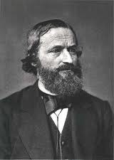
(1824-1887)
The first observation is concerned with the current flow across nodes, i.e. points in a circuit where multiple wires are connected. We invoke our pipe analogy again: If three water pipes are joined, the sum of the flow rates of the incoming water is equal to the flow rate of the outgoing water. Figure 1.5 illustrates the analogy for a joint of water pipes and a node of electrical wires.

Figure 1.5: What goes in must come out: the flow of water is conserved across pipe joints (left) and, likewise, the flow of electrical charges is conserved across wire joints (right).
Figure 1.5 suggests that outgoing current \(I_3\) is the sum of the incoming currents \(I_1\) and \(I_2,\) i.e. \(I_3 = I_1 + I_2.\) If this were not true, the node would either leak or inject charges, or the charges would have to accumulate without leaving the node. Neither effect has ever been observed, because nature conserves electrical charges. Kirchhoff’s current law states this fact concisely.
Kirchhoff’s Current Law (KCL): [Charge conservation]
The algebraic sum of the currents entering a node is zero.
This law must be read with the convention of reference directions in mind. When summing up the currents at a node, we account for incoming currents with a positive sign and outgoing currents with a negative sign. The opposite accounting works as well, if applied consistently. For example, in Figure 1.5, the sum of the currents is according to KCL:
Add \(I_3\) to both sides of the equation to see that outgoing current \(I_3\) is the sum of the incoming currents \(I_1 + I_2.\) Multiply both sides of the equation with \(-1,\) and we see that counting incoming currents as negative and outgoing currents as positive yields the same result, \(-I_1 - I_2 + I_3 = 0.\) Since KCL applies to the reference directions of the currents, the actual currents may still flow in the opposite direction. For instance, if we happen to measure currents \(I_1 = 5 A\) and \(I_3 = 2 A,\) then KCL tells us that \(I_2 = I_3 - I_1 = -3 A.\) Thus, current \(I_2\) is actually flowing out of the node rather than in.
The concept of a node in an electrical circuit is important. In fact, as used in KCL, node has a broader meaning than just a connection of wires, like those that we mark with a fat dot. Consider the circuits in Figure 1.6, two resistors in series on the left, and two parallel resistors on the right.

Figure 1.6: KCL applies to nodes that are closed surfaces.
What is the relation between currents \(I_1\) and \(I_2\) in these two circuits? In the series composition on the left, we connect resistors \(R_x\) and \(R_y\) at node \(N_2.\) Applying KCL to node \(N_2,\) we find that \(I_x + I_y = 0,\) or \(I_x = -I_y.\) No surprise here, because our node is nothing but a dot that we attached to the wire. There can be only one current flowing in one direction through the wire. Whether we call it \(I_x\) or \(I_y\) does not matter. By the same argument, if \(I_x\) is the current through resistor \(R_x,\) then \(I_1\) is the same current, i.e. \(I_1 = I_x.\) Analogously, the current through \(R_y\) is \(I_y = I_2.\) Because \(I_x = -I_y,\) we conclude that \(I_1 = -I_2.\) Notice that we could have gained this insight by applying KCL to node \(N_1,\) the closed curve around \(R_x\) and \(R_y,\) directly: the sum of the currents entering \(N_1\) must be zero, i.e. \(I_1 + I_2 = 0.\)
For the parallel composition in Figure 1.6 on the right, we suspect that \(I_1 = -I_2\) as well, because this is the consequence of applying KCL to node \(N_1.\) The circuit contains two simple nodes, \(N_2\) and \(N_3.\) This is a more complex situation than the series composition. So, let’s double check whether KCL holds for node \(N_1.\) Applying KCL at nodes \(N_2\) and \(N_3,\) we find
To find the relation between \(I_1\) and \(I_2\) we can eliminate \(I_x\) and \(I_y\) algebraically. From the equation for \(N_2,\) we have \(I_x + I_y = I_1.\) Substituting in the equation for \(N_3,\) we obtain \(I_2 + I_1 = 0,\) which is the same equation that we obtain by applying KCL to node \(N_1.\) We have just verified that KCL applies to nodes that are closed curves through a circuit. In fact, KCL applies to nodes that are arbitrary closed surfaces in 3-dimensional space as well. A large node collapsed into a small dot has the appearance of a simple node and the same electrical behavior from the perspective of the surrounding circuit.
1.3.2. Kirchhoff’s Voltage Law
The second observation of Kirchhoff characterizes the forces in a loop. A loop is a closed path through a circuit that visits each element no more than once. First consider the fluid flow analogy in Figure 1.7 with a system of three water tanks connected via pipes. If the pump is off, the height of the water columns causes a balancing flow. Since \(h_1 > h_2,\) there will be a positive flow \(U_2.\) Also, since \(h_2 > h_3,\) flow \(U_3\) will be positive. If the pump is switched on, a positive flow \(U_1\) will replenish tank 1, i.e. increase \(h_1,\) while depleting tank 3, i.e. decreasing \(h_3.\)

Figure 1.7: The flow of water through a system of connected water tanks and a pump.
The driving force behind the water flow is the hydrolic pressure caused by the height difference of neighboring water columns and of the pump. If we sum up the height differences along the loop, we find that the sum is zero:
Kirchhoff’s voltage law expresses the analogous effect for loops in electrical circuits.
Kirchhoff’s Voltage Law (KVL): [Energy conservation]
The algebraic sum of the voltages around a circuit loop is zero.

Figure 1.8: Illustration of Kirchhoff’s voltage law.
Figure 1.8 shows the circuit analogon to the water tank system in Figure 1.7. The circuit consists of a single loop with a voltage source, and three resistors. A voltage source is an idealized circuit element that generates constant voltage \(V\) with the annotated polarity, independent of the current flowing through it. We have chosen a clockwise reference direction for current \(I,\) and have annotated the polarities for the voltages across the resistors to decrease in the direction of the current. To form the sum of the voltages, assign a direction in which to traverse the loop, and account for device voltages in the direction of the loop as positive and voltages against the loop as negative. Our choice for the traversal direction is clockwise, as indicated by the blue arrow. The voltage decreases across each resistor in traversal direction, whereas the voltage increases across the voltage source. Therefore, the sum of the voltages is zero according to KVL:
Adding \(V\) to both sides shows that \(V = V_1 + V_2 + V_3,\) i.e. the driving force, the voltage source, produces voltage \(V\) that equals the sum of the voltage drops across the resistors. Thus, the electrical energy produced by the source is transformed into thermal energy by the three resistors. In other words, the circuit loop conserves energy by consuming the same amount of electrical energy as it produces. This insight is the crux behind KVL.[2]
The choice of the reference directions for voltages and currents, and the traversal direction of the loop does not affect the validity of KVL. It merely causes signs to change consistently. For example, had we chosen a counterclockwise traversal direction when applying KVL to the circuit in Figure 1.8, we would have obtained \(V - V_1 - V_2 - V_3 = 0.\) This equation is equivalent to the original KVL equation, as multiplication of both sides by \(-1\) reveals.
The concept of a loop in a circuit is easy. However, finding all loops of a circuit can be less than trivial. Consider the circuit in Figure 1.9.

Figure 1.9: KVL applies to loops that may cross wires.
The simple loops are shown on the left. Loops are simple if they do not cross wires.[3] Applying KVL to the three simple loops yields three equations:
We can form larger loops by combining these simple loops. Merging loops \(L_2\) and \(L_3\) yields loop \(L_4,\) and merging all three loops \(L_1,\) \(L_2,\) and \(L_3\) yields loop \(L_5.\) The corresponding KVL equations are:
The circuit has two more loops yet, shown on the right in Figure 1.9. Loop \(L_6\) is the result of merging loops \(L_1\) and \(L_2,\) and loop \(L_7\) merges loops \(L_1\) and \(L_3.\) Their KVL equations are:
The equations for loops \(L_1,\) \(L_2,\) and \(L_3\) relate the five voltages of the circuit to each other. From loop equations \(L_1\) and \(L_3\) we know that \(V_1 = V\) and \(V_3 = V_4.\) Furthermore, from loop \(L_2\) we can derive with the aid of \(L_1\) that \(V_2 = V_3 + V.\) Note that relative to this knowledge, the merged loop equations do not add any new information. For example, loop equation \(L_4\) is equivalent to \(L_2,\) if we employ \(L_3\) to substitute \(V_3\) for \(V_4.\) Analogously, loop equations \(L_5\) and \(L_6\) are equivalent to \(L_2\) by substituting \(V_1\) for \(V\) due to \(L_1.\) Moreover, equation \(L_7\) is equivalent to the sum of equations \(L_1\) and \(L_2.\) In general, we find that the simple loops contain all the relevant information about the voltages and energy distribution across a circuit. Nevertheless, KVL applies to all loops in a circuit.
Derive the node equations of KCL to determine the unknown currents in these circuits:

Deduce currents \(I_1\) and \(I_2\) in the 2-node circuit on the left and currents \(I_3,\) \(I_4,\) and \(I_5\) in the 3-node circuit on the right.
Consider the 2-node circuit first. We wish to determine current \(I_1\) flowing from the node on the left, call it \(N_1,\) to the node on the right, say \(N_2,\) and current \(I_2\) which exits node \(N_2.\) Node \(N_1\) has one current of \(5 A\) entering and four currents exiting. Since \(I_1\) is the only unknown current of \(N_1,\) applying KCL enables us to determine \(I_1\) by setting the sum of the currents to \(0\) or, to be mathematically precise, to \(0 A,\) because currents have unit Ampere:
Solving for \(I_1\) yields
Now that we know \(I_1,\) we find that \(I_2\) is the only unknown current of node \(N_2.\) The node equation for \(N_2\) due to KCL is:
Solving for \(I_2\) and substituting \(I_1 = -1 A\) yields
Next, we determine unknown currents \(I_3,\) \(I_4,\) and \(I_5\) of the 3-node circuit. KCL gives us three node equations, starting at the top node in clockwise direction:
The third equation is the only one with a single unknown, and permits computing \(I_5\):
Substituting \(I_5\) in the second equation yields \(I_4\):
Using the first equation, we obtain
Derive the loop equations of KVL to determine the unknown voltages in these circuits:

Deduce voltages \(V_1\) and \(V_2\) in the 2-loop circuit on the left and voltages \(V_3,\) \(V_4,\) and \(V_5\) in the 3-loop circuit on the right.
First, we deduce voltages \(V_1\) and \(V_2\) of the 2-loop circuit on the left. The circuit has two simple loops. Imagine we traverse the left loop in clockwise direction. The voltage source generates \(4 V\) in counterclockwise direction, whereas the reference directions of all three resistors point clockwise from high to low voltage. KVL yields the loop equation by forming the sum of the voltages, with those voltages negated that point against the loop direction, and setting the sum to \(0\) or, to be mathematically precise, to \(0 V,\) because voltages have unit Volt:
We rearrange the equation to obtain unknown voltage \(V_1\):
Knowing that \(V_1 = 0 V,\) we apply KVL to the simple loop on the right of the circuit to determine unknown voltage \(V_2.\) Let’s traverse the loop counterclockwise. Then the loop equation is:
so that
The circuit on the right has three simple loops. We determine voltages \(V_3,\) \(V_4,\) and \(V_5\) by applying KVL to each simple loop in clockwise direction, resulting in the three loop equations:
The first equation yields
the second equation
and substituting \(V_4\) in the third equation
You may verify that the resulting voltages fulfill KVL not only for the simple loops but all others as well.
Determine the voltages and currents of all voltage sources and resistors by applying Ohm’s law, KCL, and KVL.

Furthermore, verify that the circuit as a whole conserves energy, that is the sum of the energy consumptions of all devices is zero.
We begin the analysis of the circuit by introducing names for all unknown voltages and currents. Each of the five resistors is associated with a voltage, that we call \(V_1, V_2, \ldots, V_5.\) The circuit has two nodes, \(N_1\) and \(N_2,\) where three wires join. We denote the associated currents \(I_1,\) \(I_2,\) and \(I_3.\) The directions of all voltages and currents are chosen arbitrarily.

We apply KCL to node \(N_1,\) by counting entering currents \(I_1\) and \(I_2\) as positive and exiting current \(I_3\) as negative. Thus, we obtain node equation \(I_1 + I_2 - I_3 = 0,\) and we find that
If we apply KCL to node \(N_2,\) we obtain \(I_3 - I_1 - I_2 = 0,\) which is equivalent to the result for node \(N_1\) and, therefore, is not useful. The circuit has two simple loops, \(L_1\) and \(L_2,\) to each of which we apply KVL in clockwise direction:
The relationship between current and voltage of a resistor is given by Ohm’s law. We account for the directions by counting a current positive if it has the same direction as the voltage, otherwise we count the current as negative. Ohm’s law gives us one equation for each of the five resistors:
Substituting the resistor equations and the node equation into the loop equations yields two equations in two unknown currents \(I_1\) and \(I_2\):
Solving this system of equations yields currents:
Using the node equation we find \(I_3 = I_1 + I_2 = 0.538 A.\) Substituting these currents in the resistor equations yields the voltages:
Next, we verify these results by checking that the circuit conserves energy. Since voltage sources produce electrical energy and resistors consume electrical energy, we wish to know whether the energy transfer from the voltage sources to the resistors is confined to these devices, i.e. no energy is lost or accumulated over time. Hence, we verify whether the average energy produced per unit of time equals the average energy consumed per unit of time. In other words, the sum of the power consumptions of all devices must be zero, if we observe the passive sign convention. The power of a voltage source and of a resistor is the product of its voltage and current, \(P = V I.\) For the three voltage sources of the circuit, we count the currents negatively, because they point in the opposite direction as the voltages. Thus, we obtain the total produced power as a negative number:
Analogously, we find for the resistors:
Since the sum of the consumed and produced power is zero, the circuit conserves energy, as it should. Furthermore, we have verified the voltages and currents of our circuit analysis, because they confirm that the circuit conserves energy indeed.
1.4. Resistive Circuits
A resistive circuit consists of resistors, wires, and voltage sources. The laws of Ohm and Kirchhoff suffice to determine the voltages and currents through all of these devices. In the following, we analyze resistive circuits, and demonstrate how to exploit the gained knowledge by replacing complex with simpler equivalent circuits, and how to design circuits that divide voltages and currents.
1.4.1. Resistors in Series
We build larger circuits from smaller ones. One basic composition pattern is the series composition of two resistors. Figure 1.10 shows a circuit with a voltage source and two resistors in series.

Figure 1.10: Resistors in series.
Resistor \(R_1\) is connected to the voltage source at node \(N_1\) and to resistor \(R_2\) at node \(N_2,\) which is connected to the voltage source at node \(N_3.\) We analyze the circuit by applying KCL to the three nodes:
which tells us that \(I = I_1 = I_2.\) Not unexpectedly, the same current flows through all devices of the circuit. Next, we apply KVL to the only loop of the circuit:
At last, we invoke Ohm’s law, to obtain the relations between the resistor voltages and currents:

Substituting \(V_1\) and \(V_2\) into the KVL equation and using current \(I,\) we obtain
Observe that this equation has the form of Ohm’s law. If we interpret the sum \(R_1 + R_2\) as the resistance of a single resistor \(R_s = R_1 + R_2,\) then we can replace the resistors in series with a single resistor, and obtain an equivalent circuit shown in Figure 1.11. By KVL, the voltage across \(R_s\) is supply voltage \(V\) and, by Ohm’s law, the current is \(I = V/R_s = V/(R_1 + R_2),\) just as in the original circuit.
The idea of an equivalent circuit is useful for the analysis of larger circuits. In particular, a circuit with \(N\) resistors in series is equivalent to a circuit with a single resistance that is the sum of the series resistances:
The circuit in Figure 1.10 is a voltage divider that divides voltage \(V\) in direct proportion to the series resistances \(R_1\) and \(R_2.\) Given current \(I = V/(R_1 + R_2),\) we find the voltages across the resistors using Ohm’s law:
Thus, we can use two resistors in series to obtain two smaller voltages from a larger voltage. For example, we do not even have to know the current flowing through the circuit to find two resistors that halve voltage \(V\): choose \(R_1\) and \(R_2\) to be equal. Then, \(V_1 = R_1/(R_1 + R_1) = V/2\) and \(V_2 = R_2/(R_2 + R_2) = V/2,\) i.e. \(V_1 = V_2 = V/2.\)
Resistor 1: Resistor 2:
Explore the voltage divider by varying the resistances, and verify your findings algebraically:
- What are the voltages if the resistance ratio is \(R_1/R_2 = 1/2\)?
- What are the voltages if the resistance ratio is \(R_1/R_2 = 1/99\)?
- Which resistances cause \(I = 20 mA\) at ratio \(R_1/R_2 = 1\)?
1.4.2. Resistors in Parallel
The other basic composition pattern besides series composition is parallel composition. Figure 1.12 shows a circuit with two parallel resistors and a voltage source.

Figure 1.12: Resistors in parallel.
Both resistors \(R_1\) and \(R_2\) are connected to the voltage source at nodes \(N_1\) and \(N_2.\) By Ohm’s law, the voltage across \(R_1\) is \(V_1 = R_1 I_1,\) and the voltage across \(R_2\) is \(V_2 = R_2 I_2.\) To analyze the circuit, we first apply KVL to the two simple loops:
We find that \(V_1 = V_2 = V,\) i.e. the voltage across each of the resistors equals supply voltage \(V.\) Next, we apply KCL to node \(N_1\):

We replace \(I_1 = V_1/R_1\) and \(I_2 = V_2 / R_2\) according to Ohm’s law. Furthermore, since \(V_1 = V_2 = V,\) the node equation is equivalent to:
This equation has the form of Ohm’s law, if we interpret
as the resistance of a single resistor \(R_p.\) The equivalent circuit is shown in Figure 1.13.
The algebra above simplifies by using conductances instead of resistances. Let \(G_1 = 1/R_1\) and \(G_2 = 1/R_2,\) then Ohm’s law yields \(I_1 = G_1 V\) and \(I_2 = G_2 V,\) and the KCL equation for node \(N_1\) becomes:
Now, interpret \(G_p = G_1 + G_2\) as the conductance of the resistor in Figure 1.13, i.e. \(G_p = 1/R_p.\)
In general, if a circuit has \(N\) parallel resistors, it is equivalent to a circuit with a single conductance that is the sum of the parallel conductances:
or, in terms of resistances:
The circuit in Figure 1.12 is a current divider that divides current \(I\) in direct proportion to the conductances \(G_1\) and \(G_2,\) or in inverse proportion to their resistances \(R_1\) and \(R_2.\) From KCL and Ohm’s law, we know that
Now, express currents \(I_1\) and \(I_2\) in terms of \(I,\) \(R_1\) and \(R_2\):
These equations tell us that we can use two parallel resistors to obtain two smaller currents from a larger current. For example, to divide a current in half, use two resistors with equal resistances \(R_1 = R_2.\) Then, \(I_1 = R_2/(R_2+R_2) I = I/2\) and \(I_2 = R_1/(R_1+R_1) I = I/2,\) i.e. \(I_1 = I_2 = I/2.\)
Resistor 1: Resistor 2:
Explore the current divider by varying the resistances, and verify your findings algebraically:
- Which resistances cause \(I = 200 mA\) at ratio \(R_1/R_2 = 1\)?
- What are the currents if the resistance ratio is \(R_1/R_2 = 1/100\)?
- What are the currents \(I_1\) and \(I_2\) if the resistance ratio is \(R_1/R_2 = 1/2\) and \(I = 50 mA\)?
The current divider nourishes the widespread intuition that electricity follows the path of least resistance.
1.4.3. Resistor Networks
The concepts of voltage and current dividers are useful not only for the synthesis of circuits, but also for analyzing larger circuits with resistor networks. Example 1.7 illustrates how we can exploit the properties of series and parallel compositions for circuit analysis.

Figure 1.14: An example of a larger resistive circuit.
Consider the resistive circuit in Figure 1.14. We wish to determine voltage \(V_3\) across resistor \(R_3.\)
We could analyze the circuit by applying Ohm’s law, KCL and KVL, or, alternatively, derive an equivalent circuit that collapses the eight resistors into a single resistor. The idea of deriving an equivalent resistance is straightforward to apply. Iterate alternating steps of combining series and parallel resistors into equivalent resistors until the network is collapsed into a single resistance. Then, work backwards dividing voltages in series and currents in parallel compositions to determine the desired quantities.
Figure 1.15 below collapses the resistor network of Figure 1.14 into an equivalent resistance \(R_{30}.\) In the first step, we introduce equivalent resistances for all series compositions in the branches of the circuit in Figure 1.14:
In the second step, we replace parallel resistors \(R_{11},\) \(R_5,\) and \(R_{12}\) with equivalent resistance
In the third step, we collapse series resistors \(R_{10}\) and \(R_{20}\) into \(R_{30} = R_{10} + R_{20}.\) The resulting equivalent circuit enables us to determine current \(I = V/R_{30}\) that flows through the series-parallel resistor network as a whole.

Figure 1.15: Transformation into equivalent circuit.
Next, we work backwards through the transformations to determine \(V_3.\) Current \(I\) flows not only through \(R_{30}\) but also through each of the series resistors \(R_{10}\) and \(R_{20}.\) Expanding \(R_{20}\) into three parallel resistors, we find that current \(I\) divides into three branches. We are interested in the current through \(R_{11}\) only:
because the desired voltage \(V_3\) is the voltage induced by \(I_{11}\) across \(R_3\): \(V_3 = R_3 I_{11}.\) Substituting the intermediate expressions yields \(V_3\) as an unwieldy function of \(V\) and resistors \(R_1\) through \(R_8\):
Try deriving \(V_3\) using KCL, KVL, and Ohm’s law rather than calculating equivalent resistances to decide which method you prefer.
Compute the equivalent resistances \(R_s,\) \(R_p,\) and \(R_{sp}\) in \(k\Omega.\)

The series composition of resistors \(R_1\) and \(R_2\) has equivalent resistance:
\[R_s = R_1 + R_2 = 1\,k\Omega + 2\,k\Omega = 3\,k\Omega\,.\]The parallel composition of resistors \(R_1\) and \(R_2\) has equivalent conductance:
\[\begin{eqnarray*} G_p &=& G_1 + G_2 \\ \frac{1}{R_p} &=& \frac{1}{R_1} + \frac{1}{R_2} \\ &=& \frac{1}{1\,k\Omega} + \frac{1}{2\,k\Omega} \\ &=& \frac{3}{2\,k\Omega} \\ R_p &=& \frac{2}{3}\,k\Omega\,. \end{eqnarray*}\]We analyze the series-parallel composition of resistors inside-out. The series composition of \(R_1\) and \(R_2\) has equivalent resistance:
\[R_{1,2} = R_1 + R_2 = 3\,k\Omega\,.\]This resistance is in parallel with \(R_3.\) Their equivalent resistance is
\[R_{1,2,3} = \frac{R_{1,2}\,R_3}{R_{1,2} + R_3} = \frac{3}{2}\,k\Omega\,.\]This resistance is in series with \(R_4.\) The resulting equivalent resistance is
\[R_{sp} = R_{1,2,3} + R_4 = 2\,k\Omega\,.\]
Audio amplifiers use a potentiometer to control the volume of the loudspeaker. A potentiometer is a voltage divider that consists of a resistor \(R\) with an adjustable tap to partition \(R\) into \(R_1\) and \(R_2\) such that \(R = R_1 + R_2.\) The audio amplifier supplies output voltage \(V_a\) to the potentiometer, and the volume control taps voltage \(V_s\) for the speaker amplifier. The larger \(V_s,\) the louder is the sound produced by the speaker.

Plot voltage \(V_s\) as a function of the potentiometer position represented by \(R_2.\) Assume the speaker amplifier has an input resistance of \(50 \Omega,\) the potentiometer has resistance \(R = 1 k\Omega,\) the tap permits adusting \(R_2\) within range \(0 \Omega \le R_2 \le R,\) and the audio amplifier supplies voltage \(V_a = 2 V.\)
The circuit diagram on the right shows the potentiometer with input voltage \(V_a = 2V\) and the speaker amplifier replaced by its input resistance of \(50 \Omega.\) We wish to derive \(V_s\) as a function of \(R_2.\)

We perform a circuit analysis. We know that \(R = R_1 + R_2\) and \(R = 1 k\Omega.\) Since we treat \(R_2\) as a free variable that represents the potentiometer position, we express \(R_1\) as a function of \(R_2\):
Voltage \(V_s\) drops off both resistances \(R_2\) and the \(50 \Omega\) input resistance of the speaker amplifier. To simplify the circuit, we replace these two parallel resistors with their equivalent resistance
Now, series resistors \(R_1\) and \(R_p\) form a vanilla voltage divider. From Example 1.5 we know that
Substituing \(R_1\) and \(R_p,\) we find \(V_s\) as a function of \(R_2\):
The plot shows \(V_s\) as a function of \(R_2\):

Voltage \(V_s\) increases monotonically in \(R_2.\) However, it increases nonlinearly. This behavior offers the human user quite a natural feel. The potentiometer acts much more sensitive to changes at low volumes than at high volumes, giving you finer control over low volumes.
Determine the equivalent resistances between terminals A-B, A-C, and B-D, respectively.

We demonstrate how to determine the equivalent resistance if two terminals span a resistor network that is a series-parallel composition, i.e. the network is constructed by repeated application of series or parallel composition of series-parallel subnetworks. First we redraw the network to expose the series and parallel compositions and, second, we collapse the network into a single resistor by step-wise replacement of series or parallel compositions with equivalent resistances. The key is to redraw the circuit so that we can easily see which compositions are series and which are parallel.
We begin with the equivalent resistance between terminals A and C. Remove terminals B and D, and imagine you pull terminal A to the left and terminal C to the right. Then, the circuit resembles this schematic:

This schematic shows that the network between terminals A and C is a parallel composition of three subnetworks. The top and bottom subnetworks are series compositions of two resistances, respectively, and the subnetwork in the middle is trivial because it consists of a single resistor only. We replace the simple series compositions first. The equivalent resistance of \(R_1\) and \(R_2\) is:
and, analogously:
Proceding with the parallel composition of \(R_{1,2},\) \(R_5,\) and \(R_{3,4},\) we form the sum of the reciprocals and obtain resistance \(R_{A\text{-}C}\) as a function of resistances \(R_1, \ldots, R_5\):
In the special case where all resistances are equal, for example \(R_1 = R_2 = \ldots = R_5 = R = 10 k\Omega,\) the expression for \(R_{A\text{-}C}\) simplifies dramatically to
Next, we consider the equivalent resistance between terminals A and B. We remove terminals C and D and redraw the circuit imagining we pull terminal A to the left and terminal B to the right:

The circuit is a series-parallel composition of resistors. We compute the equivalent resistance by replacing subcircuits, working inside-out. We note that \(R_3\) and \(R_4\) are composed in series, and replace the two resistors with equivalent resistance \(R_{3,4} = R_3 + R_4.\) Now, \(R_5\) and \(R_{3,4}\) are composed in parallel. We replace the parallel composition with equivalent resistance \(R_{3,4,5},\) which we compute by adding the reciprocals:
At this point, we note that \(R_{3,4,5}\) and \(R_2\) form a series composition. Thus, we replace the bottom branch of the circuit with equivalent resistance \(R_{2,3,4,5} = R_{3,4,5} + R_2.\) This leaves us with a parallel composition of \(R_1\) and \(R_{2,3,4,5},\) and equivalent resistance
For comparison, in the special case where where all resistances are equal to \(R = 10 k\Omega,\) the expression for \(R_{A\text{-}B}\) simplifies to
The resistance between terminals B and D requires a circuit analysis with KCL, KVL, and Ohm’s law, because the resistor network is not a series-parallel composition. No matter how you push or pull, resistor \(R_5\) forms a bridge between the two parallel branches \(B\text{-}R_1\text{-}R_3\text{-}D\) and \(B\text{-}R_2\text{-}R_4\text{-}D\) that cannot be generated with a series or parallel composition. The solution of the circuit analysis (try it yourself!) is:
Again, for comparison, in the special case where where all resistances are equal to \(R = 10 k\Omega,\) the expression for \(R_{B\text{-}D}\) simplifies to
What are the equivalent resistances between any of the other terminal pairs?
You have a voltage source with \(6 V\) and an unlimited supply of \(10 k\Omega\) resistors. Design resistive circuits to generate voltage \(V_a = 2 V,\) \(V_b = 3 V,\) \(V_c = 4 V,\) and \(V_d = 5 V,\) respectively.
Our plan is to design voltage divider circuits, because each of the desired voltages is less than supply voltage \(V = 6 V.\) We pick the simplest voltage first, \(V_b = 3 V,\) because \(V_b\) is exactly half of \(V.\) Analogous to Example 1.5, we compose two resistors \(R_1\) and \(R_2\) in series, where \(R_1 = R_2 = R = 10 k\Omega.\) Then, we can tap \(V_b\) off either resistor, because
The corresponding voltage divider circuit is shown on the left:

Next, we design a circuit to divide \(V = 6V\) down to \(V_a = 2V.\) We note that \(V_a\) is one third of \(V,\) and observe in the corresponding voltage divider equation
that we wish to determine \(R_x\) and \(R_y\) such that
Simplify this equation, and we find the equivalent condition \(R_y = 2 R_x.\) This condition is easy to fulfill: if we choose \(R_x = R,\) then \(R_y = 2 R,\) which we implement as a series composition of two resistors with resistance \(R.\) The resulting voltage divider circuit consists of three series resistors, as shown in the middle of the figure above. Note that each of the three resistors has a voltage drop of \(2 V\) or one third of \(6 V.\) Thus, we can tap \(V_a = 2 V\) off each of the resistors. Also note that this voltage divider circuit can be used to generate \(V_c = 4 V\) as well, because \(V_c = 2 V_a.\) Thus, we obtain \(V_c\) at the terminals of the series composition of two resistors, either \(R_1\) and \(R_2\) because \(V_1 + V_2 = 4 V\) or \(R_2\) and \(R_3\) because \(V_2 + V_3 = 4 V.\)
Voltage \(V_d = 5 V\) can be generated with an analogous argument as \(V_a.\) Since \(V_d/V = 5/6,\) we deduce from the voltage divider equation that \(R_x = 5 R_y.\) Therefore, if we choose \(R_y = R,\) then \(R_x = 5 R,\) which we could implement with six series resistors of resistance \(R.\) An alternative circuit derives from the voltage divider equation by choosing \(R_x = R.\) Then, \(R_y = R / 5,\) which we can implement with five parallel resistors of resistance \(R\) because the equivalent resistance \(R_p\) is
The corresponding voltage divider circuit is shown on the right in the figure above.
1.5. RC Circuits
In this section we introduce the capacitor and discuss RC circuits, circuits with resistors and capacitors. The usefulness of RC circuits unfolds when voltages and currents change over time. Then, RC circuits exhibit more interesting behavior than resistive circuits, and require mathematical tools from calculus for transient analysis.
1.5.1. The Capacitor
(1791-1867)
A capacitor is an electrical device with capacitance \(C.\)[4] The unit of capacitance is the Farad, \(1 F = 1 C / V,\) i.e. one Coulomb per Volt, in honor of the English physicist Faraday.

Figure 1.16: Capacitor with current and voltage.
Capacitors store energy in an electrical field. The charge \(q\) in the capacitor is proportional to the voltage \(v\) across the field:
A capacitor consists of a dielectric insulator sandwiched between two conducting plates. Dielectrics are materials that do not conduct electric current but polarize in an electrical field, e.g. porcelain or oil. The capacitance of a capacitor is
where \(A\) is the area of the plates, \(d\) is the thickness of the dielectric, and \(\epsilon\) is a material constant of the dielectric. The larger a capacitor, the more charge it can store, and the larger is its capacitance.
When applying a constant voltage \(v\) to a capacitor, it behaves like an insulator, because the dielectric isolates the terminals. No current flows through the capacitor. However, if the voltage varies over time, the capacitor serves as an energy reservoir. The time dependence makes the behavior of a capacitor much harder to describe than a resistor but the usefulness of its properties are worth the effort.
Assume voltage \(v(t)\) across a capacitor with capacitance \(C\) varies over time \(t.\) Then, charge \(q(t)\) on the capacitor varies proportionally:
Since current is the change of charge over time, \(i(t) = d q(t) / dt,\) the current through the capacitor is
Alternatively, we use the integral form to express \(v(t)\) as a function of \(i(t)\):
The energy stored in the capacitor at time \(t\) is the integral of the power consumption over time:
Here, we assume that the integration constant is zero, as it would be if the initial voltage were zero. Unlike a resistor, which dissipates electrical energy as heat, a capacitor stores electrical energy. At any point in time, the amount of energy stored in a capacitor represents the history of changes accumulated by the integral. In contrast, the energy consumed by a resistor is instantaneous and independent of the history. Therefore, capacitors enable us to build memories whereas resistors alone do not.
1.5.2. Capacitor Networks
The two basic types of composition, series and parallel, are useful for constructing and analyzing larger capacitor networks. Figure 1.17 shows two capacitors in series and a voltage source.

Figure 1.17: Capacitors in series.
To analyze the series composition, we observe that current \(i(t)\) flows through both capacitors \(C_1\) and \(C_2.\) Applying KVL to the circuit loop, we find that
Observe that the last expression gives the voltage across a single capacitor with capacitance \(C_s,\) such that
Thus, the equivalent capacitance of two capacitors in series is calculated analogously to the equivalent resistance of two parallel resistors. In general, the equivalent capacitance \(C_s\) of \(N\) capacitors in series is

Figure 1.18: Capacitors in parallel.
The parallel composition of two capacitors is shown in Figure 1.18. We notice that the voltages across the capacitors are \(v_1 = v_2 = v.\) Applying KCL, we obtain:
Observe that this expression characterizes the current through a single capacitor with capacitance \(C_p,\) where
The capacitances of two parallel capacitors are additive. This is consistent with the geometric intuition that the areas of capacitor plates add up when joined. In general, the equivalent capacitance \(C_p\) of \(N\) parallel capacitors is the sum
The concept of equivalent capacitances enables us to simplify larger capacitive networks without need for calculus, analogous to the simplification of resistive networks in Example 1.7.
1.5.3. Steady State vs Transients

Figure 1.19: Resistive circuit.
We say that a circuit is in steady state if all voltages and currents are stable.[5] For example, when the resistive circuit in Figure 1.19 is in steady state, the resistor conducts current \(i\) according to Ohm’s law. According to KVL, we have \(v_R = V,\) and
Since currents and voltages do not change over time in steady state, we emphasize the situation by using upper-case letters \(I = i(t)\) and \(V = v(t).\)

Figure 1.20: Capacitive circuit.
The steady state behavior of the capacitive circuit in Figure 1.20 is even simpler than that of the resistive circuit. By KVL, we have \(v_C = V.\) Since the voltage across the capacitor is constant, the capacitor isolates its terminals, such that no current can flow. Therefore, we conclude that the steady state current is
independent of the magnitude of capacitance \(C.\)
The interesting behavior of the capacitive circuit is not its steady state but its transient behavior. When the voltage of the voltage source varies over time, e.g. if we could switch the voltage on or off, the circuit reacts with a transient response. We can describe the transient response of a circuit using methods from calculus. In the next section, we perform the transient analysis of an RC circuit.
1.5.4. RC in Series

Figure 1.21: RC series circuit.
One of the simplest RC circuits is the series composition of a resistor and a capacitance, as shown in Figure 1.21. In steady state, when the voltage source supplies constant voltage \(V,\) the capacitor acts like an insulator. No current can flow through the circuit loop, including the resistor. Therefore, by Ohm’s law,
because \(I = 0\) in steady state, and by KVL
To study the transient behavior of the RC circuit, we introduce a new device, a switch, that we can open or close. The open switch disconnects its terminals, whereas the closed switch behaves like a wire that connects the terminals. Figure 1.22 extends the circuit of Figure 1.21 with a switch. We assume that the switch is open initially, and we close the switch at time \(t=0.\) We analyze the time dependent response of the circuit to the closing of the switch.

Figure 1.22: RC circuit with switch.
\(t < 0\): Switch is open.
The open switch prevents a current from flowing through the circuit. Therefore, \(i(t) = 0\) and, by Ohm’s law, \(v_R(t) = R\, i(t) = 0.\) Since the \(+\) terminal of the capacitor floats, i.e. is not connected to any device that could induce a particular voltage, we assume that \(v_C(t) = 0.\)
\(t \ge 0\): Switch is closed.
We apply KVL to the circuit loop in clockwise direction:
\[R i(t) + \frac{1}{C} \int_0^t i(\tau) d\tau - V = 0\,,\]and transform the integral equation into a differential equation by taking the derivative in \(t\):
\[R \frac{d i(t)}{dt} + \frac{1}{C} i(t) = 0\,.\]This equation models the time dependent behavior of current \(i\) through the RC circuit. Dividing both sides by \(R\) casts the equation into the form of a homogeneous differential equation with constant coefficients, actually one constant coeffient \(1/RC\):
\[\frac{d i(t)}{dt} + \frac{1}{R C} i(t) = 0\,.\]Recall from calculus that such an equation has the general solution
\[i(t) = k_1 + k_2 e^{-k_3 t}\,,\]where \(k_1,\) \(k_2,\) and \(k_3\) are constants that are determined by the initial condition at time \(t=0\) and the steady state, where \(t \rightarrow \infty.\)
\(t \rightarrow \infty\): steady state
In steady state with a closed switch, the circuit behaves as analyzed above for Figure 1.21 already. The capacitor acts like an insulator, so that \(i(\infty) = 0.\) Because \(e^{-k_3 t} \rightarrow 0\) for \(t \rightarrow \infty,\) the steady state enables us to determine constant \(k_1\):
\[\begin{split}\begin{eqnarray*} i(\infty) &=& k_1 + k_2 \cdot 0 \\ \Leftrightarrow\qquad k_1 &=& 0\,. \end{eqnarray*}\end{split}\]\(t = 0\): initial condition
The switch has just closed. Therefore, no charges can have accumulated in the capacitor yet, so that \(v_C(0) = 0.\) Hence, by KVL, source voltage \(V\) equals the voltage across the resistor, \(v_R(0) = V.\) This voltage induces instantaneous current \(i(0) = V/R\) through the resistor. We call this current \(I_0 = V/R\) at \(t=0\) the initial current. Since \(e^0 = 1,\) we can determine constant \(k_2\):
\[\begin{split}\begin{eqnarray*} i(0) &=& k_2 \cdot 1 \\ \Leftrightarrow\qquad k_2 &=& \frac{V}{R}\,. \end{eqnarray*}\end{split}\]It remains to determine constant \(k_3.\) To that end, we substitute \(i(t) = I_0 e^{-k_3 t}\) in the differential equation. Applying the chain rule of differentiation, we find that
\[\frac{d i(t)}{d t} = - k_3 I_0 e^{-k_3 t}\,,\]and the differential equation yields
\[\begin{split}\begin{eqnarray*} - k_3 I_0 e^{-k_3 t} + \frac{1}{RC} I_0 e^{-k_3 t} &=& 0 \\ k_3 &=& \frac{1}{RC}\,. \end{eqnarray*}\end{split}\]Thus, we have found the solution for current \(i(t)\) when \(t \ge 0\):
\[i(t) = I_0 e^{-\frac{t}{RC}} = \frac{V}{R} e^{-\frac{t}{RC}}\,.\]We call constant \(RC,\) the product of the resistance and capacitance, the time constant of the circuit, because it determines how fast the current approaches its steady state value \(i(\infty) = 0.\)
Now that we know current \(i(t),\) we can deduce voltage \(v_C(t)\) across the capacitor:
\[\begin{split}\begin{eqnarray*} v_C(t) &=& \frac{1}{C} \int_0^t i(\tau) d \tau \\ &=& \frac{V}{RC} \int_0^t e^{-\frac{\tau}{RC}} d \tau \\ &=& V \bigl(1 - e^{-\frac{t}{RC}}\bigr)\,. \end{eqnarray*}\end{split}\]
The interactive graph Figure 1.23 explores the dependence of \(i(t)\) and \(v_C(t)\) on time constant \(RC,\) assuming that \(I_0 = 1 A\) and \(V = 1 V.\) At time \(t=0\) the current jumps from 0 to \(I_0,\) and then decreases exponentially as time passes. This current charges the capacitor. Therefore, voltage \(v_C(t),\) which is initially 0, increases when the switch closes at time \(t=0,\) and approaches \(V = 1 V\) within a time period proportional to \(RC.\) At time \(t=0,\) a larger current increases the capacitor voltage faster than the smaller current at \(t \gg 0.\) The bottomline is that the time period the current takes to charge the capacitor is proportional to \(RC.\)
Time constant RC: 1
Figure 1.23: Capacitor voltage and current as a function of time. Vary time constant RC to see at which time \(t\) the capacitor voltage reaches \(V = 1 V,\) effectively completing the transition that starts with closing the switch at time \(t = 0.\)Compute the equivalent capacitances \(C_s,\) \(C_p,\) and \(C_{sp}\) in \(pF.\)

The series composition of capacitors \(C_1\) and \(C_2\) has equivalent capacitance \(C_s\):
\[\begin{eqnarray*} \frac{1}{C_s} &=& \frac{1}{C_1} + \frac{1}{C_2} \\ &=& \frac{1}{10\,pF} + \frac{1}{20\,pF} \\ &=& \frac{3}{20\,pF} \\ C_s &=& \frac{20}{3}\,pF\,. \end{eqnarray*}\]The parallel composition of capacitors \(C_1\) and \(C_2\) has equivalent capacitance:
\[C_p = C_1 + C_2 = 10\,pF + 20\,pF = 30\,pF\,.\]We analyze the series-parallel composition of capacitors inside-out. The series composition of \(C_1\) and \(C_2\) has equivalent capacitance:
\[C_{1,2} = \frac{C_1\,C_2}{C_1 + C_2} = 5\,pF\,.\]This capacitance is in parallel with \(C_3.\) Their equivalent capacitance is:
\[C_{1,2,3} = C_{1,2} + C_3 = 20\,pF\,.\]This capacitance is in series with \(C_4.\) The resulting equivalent capacitance is:
\[C_{sp} = \frac{C_{1,2,3}\,C_4}{C_{1,2,3} + C_4} = 10\,pF\,.\]
Compute the equivalent capacitances of these capacitive circuits, assuming each capacitor has a capacitance of \(C = 6 pF\):

We observe that all four capacitive circuits are series-parallel networks, that we discuss in Exercise 1.12 in the context of resistor networks as well.
Consider the series composition of three capacitors given in circuit (a). From our study of capacitor networks we know that the equivalent capacitance \(C_a\) of the series composition is
Therefore, we find for \(C = 6 pF\) that
Circuit (b) shows a parallel composition of three capacitors. As discussed in Section Capacitor Networks their capacitances add up to equivalent capacitance
Circuit (c) is a parallel composition of two branches, where the left branch is a series composition. We begin by replacing the series composition with its equivalent capacitance
Next, we determine equivalent capacitance \(C_c\) of the parallel composition:
This is the equivalent capacitance of circuit (c).
Circuit (d) is a series composition, where the bottom subnetwork forms a parallel composition. Again, we begin by replacing the parallel composition with its equivalent capacitance:
Then, the equivalent capacitance \(C_d\) of the series composition is
We find that the four capacitive networks have distinct equivalent capacitances. From a constructive point of view, if you happen to have a supply of capacitors with \(C = 6 pF,\) you can combine three capacitors in a series-parallel fashion to obtain capacitances of \(2 pF,\) \(4 pF,\) \(9 pF,\) and \(18 pF.\)
Consider the capacitors below, assuming the dielectric has permittivity \(\epsilon = 8 \times 10^{-10} F/m.\) The dielectric of capacitor (a) shall have thickness \(d = 8 {\mathring A}.\) Unit Angstrom is defined as \(1 {\mathring A} = 10^{-10} m.\) Furthermore, the length of capacitor (a) shall be \(L = 1 \mu m\) and its width \(W = 1 \mu m.\)

Determine the capacitances of the three capacitors.
The capacitance of a capacitor with plate area \(A = L W\) is \(C = \epsilon L W / d.\) Therefore, to determine capacitance \(C_a\) of capacitor (a), all we need to do is plug in the numbers, and obtain:
Analogously, we can determine capacitance \(C_b\) of capacitor (b) by plugging the numbers into the capacitance formula. However, notice that capacitor (b) has the same dielectric thickness as capacitor (a), and the plate area matches that of an array of \(3 \times 2\) capacitors (a). Thus, we may view capacitor (b) as a parallel composition of six copies of capacitor (a):

Since the equivalent capacitance of parallel capacitances is their sum, we find that
Capacitor (c) has four times the plate area of capacitor (a) and its dielectric is twice as thick. Therefore, we may derive capacitance \(C_c\) from \(C_a\):
such that \(C_c = 2 C_a = 2 pF.\)
The circuit below extends Figure 1.22 with a switch position that enables us to bypass the voltage source. Assume that the circuit is in the steady state after the transition discussed above, and analyze what happens after throwing the switch downward.

Before throwing the switch, the circuit has the same topology as the circuit in Figure 1.22 with the switch closed. We found above that the steady state of that circuit at \(t \rightarrow \infty\) is \(i(\infty) = 0,\) \(v_R(\infty) = 0,\) and \(v_C(\infty) = V.\) Now, we assume that our modified circuit assumes this steady state as start state, and we throw the switch downward at \(t = 0.\) Thus, for the new switch transition of interest we assume that \(i(t) = 0,\) \(v_R(t) = 0,\) and \(v_C(t) = V\) for \(t < 0.\)

After throwing the switch downward at \(t=0,\) the voltage source is disconnected, and the active part of the circuit consists of the single loop shown on the right. In the following, we analyze this circuit for \(t \ge 0.\)
Apply KVL in clockwise direction to obtain loop equation
Taking the derivative yields the differential equation
This is the same differential equation we found during the analysis of the switch transition above. However, we expect a different solution, because the initial conditions differ. In particular, the capacitor stores charges such that voltage \(v_C(0) = V,\) i.e. the inital capacitor voltage equals the voltage of the disconnected voltage source. Assuming as above that the loop current has the general solution
we conclude that \(k_1 = 0\) because \(i(\infty) = 0.\) Initial condition \(v_C(0)=V\) enforces \(v_R(0) = -V,\) or KVL would not hold at \(t = 0.\) We conclude that the initial loop current is the current through the resistor, so that
The time constant of the series composition of resistor and capacitor is \(RC,\) so that constant \(k_3\) must be \(k_3 = 1/RC.\) In summary, we have found that loop current
flows in the opposite direction of the reference direction. The capacitor acts as current source, and discharges itself through the resistor. Furthermore, we can deduce voltage \(v_C(t)\) across the capacitor directly from KVL without integration:
The capacitor voltage decreases exponentially from \(v_C(0) = V\) to \(v_C(\infty) = 0.\)
1.6. Transistors
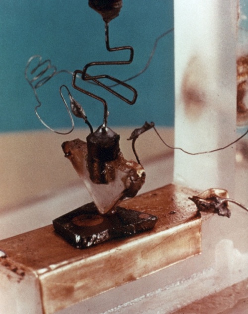
Figure 1.24: The first transistor at AT&T, 1947.
A transistor is a switching device that enables us to control the flow of current in one circuit by means of the voltage in another circuit. The first transistor prototype is shown in Figure 1.24. It was built at AT&T’s Bell Laboratories in 1947 by Bardeen, Brattain, and Shockley, see Figure 1.25. Today, transistors exist in various technologies of different types. We discuss the most common kind, the MOSFET, metal-oxide-semiconductor field-effect transistor, or MOS transistor for short. We are less interested in the inner workings of transistors but their common functionality and timing behavior. To that end, we study a simplistic switch model and a more detailed RC model of the MOS transistor.
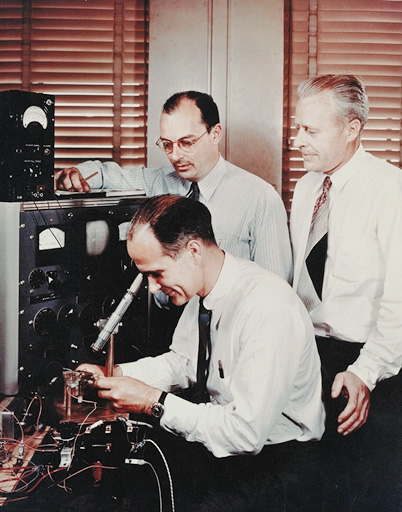
Figure 1.25: The inventors of the transistor: William Shockley (front), John Bardeen (left), and Walter Brattain (right).
1.6.1. MOS Transistors
The name MOS transistor refers to the layer structure in which transistors are built: metal on top, silicon dioxide in the middle, and a semiconductor at the bottom. MOS transistors come in two types, the nMOS and the pMOS transistor, shown in Figure 1.26.

Figure 1.26: Two types of MOS transistor: nMOS (left) and pMOS (right).
MOS transistors are devices with three terminals: gate, source, and drain. The silicon dioxide \(\text{(SiO}_2\text{)}\) serves as dielectric layer of a capacitor with the gate metal as the top plate and the silicon substrate as the bottom plate. In the nMOS transistor, the n-type source and drain regions contain donor atoms, capable of donating electrons to an electrical current, whereas the substrate is of p-type, i.e. it contains acceptor atoms that donate positive charges (holes). In the pMOS transistor, the types of the regions are reversed.

Figure 1.27: Operation of an nMOS transistor: switch open (left) and switch closed (right).
An nMOS transistor acts like a switch between source and drain, controlled by the voltage of the gate. If the gate voltage is high, source and drain are connected, i.e. the switch is closed. If the gate voltage is low, source and drain are disconnected, i.e. the switch is open. Figure 1.27 illustrates the operation of the nMOS transistor. The bulk contact connects the substrate of the nMOS transistor to low voltage. The MOS transistor disconnects source and drain if the gate is also connected to low voltage, such that the gate-substrate capacitor contains no charges. If the voltages of the source and drain are not lower than the voltage of gate and substrate, then the junctions between the n-type regions and the p-type substrate act like reverse biased diodes, that block any current from flowing across these junctions. As a result, source and drain are effectively disconnected from each other. In contrast, when the gate voltage is high, then the gate-substrate capacitor stores charges. In particular, positive charges accumulate at the gate plate and negative charges below the silicon dioxide in the substrate. These negative charges form an inversion layer of n-type inside the p-type substrate. This so-called channel connects the source and drain terminals via an n-type path. Electrons can flow through this path. If the source voltage is low and drain voltage high, the transistor acts like a closed switch with electrons flowing from source to drain, producing a current that we account for in the opposite direction.
The pMOS transistor operates analogously, except that all polarities are reversed. In particular, a pMOS transistor has the opposite switch behavior compared to an nMOS. The pMOS acts like an open switch if the gate voltage is high and like a closed switch if the gate voltage is low. The carriers of electrical current in a pMOS transistor are positive charges rather than negative charges as in an nMOS. This fact has consequences on the timing behavior, because positive charges are less mobile in a semiconductor than negative charges. As a result, a pMOS transistor can conduct only about half the current between source and drain than a nMOS transistor.

Figure 1.28: Symbols for MOS transistors: nMOS (left) and pMOS (right) with gate, source, and drain terminals.
The transistor symbols used in circuit schematics are shown in Figure 1.28. The circle on the gate of the pMOS transistor indicates that the pMOS behavior is complementary to the nMOS, depending on the voltage of the gate. These symbols emphasize that the gate is disconnected from source and drain, and forms a capacitor plate that controls the switch between source and drain.
1.6.2. Switch Model
The power of abstraction is to restrict our focus on the essential properties of interest. In case of MOS transistors, the digital abstraction restricts our focus on their discrete functionality. We abstract the voltage levels by considering two values only, high and low voltage. Denote high voltage as 1 and low voltage as 0. Then, the switch behavior of nMOS and pMOS transistors can be summarized as shown in Figure 1.29. If the gate value is 0, the nMOS transistor is off, i.e. the switch between source and drain is open, and the pMOS transistor is on, i.e. the switch between source and drain is closed. If the gate value is 1, then the nMOS transistor is on and the pMOS transistor is off. We say that nMOS and pMOS transistors behave complementary to express that their switch behaviors are opposites of each other.

Figure 1.29: Switch model of MOS transistors.
In reality, MOS transistors are neither ideal switches, nor can we apply high and low voltages to the gates only. In fact, the current between source and drain is proportional to the gate voltage, which may assume any value between high and low when transitioning between the two voltages. Thus, in reality there is no such clear distinction between on and off as idealized by the switch model. Nevertheless, the switch model does capture the discrete switch behavior and, therefore, enables us to argue about the functionality of digital circuits built with MOS transistors.
To demonstrate the usefulness of the switch model, consider the simplest MOS circuit, a series composition of nMOS and pMOS transistors in Figure 1.30.

Figure 1.30: Inverter circuit.
This inverter schematic deserves a few comments to be interpreted as intended. We assume two common conventions to simplify schematics:
We do not draw voltage sources. If we would, the inverter schematic might look like the one in Figure 1.31, where the circuit loop with the voltage source distracts the viewer from the essential part, the two transistors. Instead, we draw the high and low voltage terminals of the voltage source only.

Figure 1.31: Symbols for high and low voltage terminals of a voltage source, used to avoid cluttering schematics with supply loops like the one shown on the left.
Imagine we have voltage supply rails for high voltage at the top of a schematic and for low voltage at the bottom. We can tap the rails anywhere we want. Rather than drawing continuous lines for top and bottom rails, however, we use a T-symbol to denote high voltage supply and a \(\perp\)-symbol, T turned upside-down, for low voltage where needed, see Figure 1.30. Since it is a voltage difference that exerts an electrical force, we do not worry about absolute voltage values. Instead, we take the liberty to define the low voltage of a circuit as reference voltage, and assign value \(0 V\) to represent low. In schematics, we call this reference ground, and emphasize this reference point occasionally, for example by annotating the \(\perp\)-symbol with the text GND, or by using more distinctive symbols like the three horizontal lines or a triangle. The high voltage terminal of a voltage source is commonly also denoted as \(V_{DD},\) and occasionally used as annotation for the T-symbol.

Figure 1.32: Wiring conventions. Draw a dot if two wires are connected at their intersection. If two wires intersect without a dot, they are not connected. Wires are always assumed to be connected at T-junctions, whether we draw a dot for clarity or not.
We draw dots to indicate connectivity at wire intersections. In complex circuits we may not be able to avoid that unrelated wires cross on top of each other. To distinguish two crossing wires without connection from intersecting wires with a connection, we explicitly mark connections at wire intersections with a dot. In contrast, we assume that wires are always connected at T-junctions. For clarity, we may mark the connections with a dot. In Figure 1.30, we save the dots at the T-junctions of the supply rails as well as terminals \(A\) and \(Y.\)
With these conventions in mind, we now analyze the series composition of an nMOS and pMOS transistor in Figure 1.30 using the switch model. We note that terminal \(A\) is an input terminal that drives the gates of both transistors either to high or low voltage. Terminal \(Y\) is connected to the drain terminals of both transistors, and is the output of the circuit. To deduce output \(Y\) as a function of input \(A,\) we compile a table of all combinations of input values. Since the circuit has only one input, we can either set input \(A\) to 0, for low voltage, or to 1, for high voltage. Hence, Table 1.1 has two rows:
| A | pMOS | nMOS | Y |
|---|---|---|---|
| 0 | on | off | 1 |
| 1 | off | on | 0 |
We introduce one column for each transistor, in this case the pMOS and the nMOS transistor, and one column for each output, here output \(Y.\) We call the resulting table a switch table, because it tracks the switch positions of the transistors. If \(A=0,\) the pMOS is switched on whereas the nMOS is switched off. Conversely, if \(A=1,\) the pMOS is switched off and the nMOS is switched on. The resulting switch positions are shown in Figure 1.33 for \(A=0\) on the left and \(A=1\) on the right.

Figure 1.33: Switch operation of inverter.
Once we know the switch positions, we can derive the value of output \(Y.\) To that end, we find a path through the switches that connects output \(Y\) either to \(V_{DD}\) or to GND. In case where \(A=0,\) the pMOS is on, connecting output \(Y\) to \(V_{DD},\) whereas the nMOS off, disconnecting output \(Y\) from GND. The circuit forms a path between \(V_{DD}\) and \(Y.\) Therefore \(Y=1,\) for high voltage, as recorded in the switch table. In the other case, where \(A=1,\) the nMOS connects \(Y\) to GND whereas the pMOS disconnects \(Y\) from \(V_{DD}.\) We conclude that \(Y=0,\) representing low voltage.
If we ignore the switch positions in the switch table, and focus on input \(A\) and output \(Y\) instead, we see that the circuit outputs the inverted input. Whenever \(A=0\) then \(Y=1,\) and when \(A=1\) then \(Y=0.\) Thus, the circuit implements the function of an inverter.
1.6.3. RC Model
The switch model enables us to analyze the logical function of a MOS transistor circuit, such as the inverter in Figure 1.30. For simplicity the switch model deliberately ignores the details that govern the electrical behavior of the circuit. If we wish to know how fast a change at the input of an inverter propagates to its output, we need a different model. In the following, we extend the switch model of the nMOS transistor into an RC model that captures the timing behavior of a transistor circuit, and apply the RC model to an inverter.
Transistor RC Model
The RC model preserves the distinctive property of the nMOS transistor that the gate-substrate capacitance and the source-drain path belong to separate electrical circuits, although the voltage of the gate controls the switch behavior of the source-drain path. The second property that the RC model captures are parasitic capacitances. The dominant parasitic capacitance of an nMOS transistor is the drain-bulk capacitance \(C_{db},\) which diverts charges from the source-drain current. There is also a parasitic source-bulk capacitance, but its effect can be ignored if source and bulk are both tied to ground, which is the common case in circuit design. Parasitic capacitances are an undesirable artifact that we cannot avoid when building MOS transistors. Figure 1.34 shows the schematic of the nMOS RC model.

Figure 1.34: RC model of nMOS transistor with gate capacitance \(C_g\) and on-resistance \(R_{on}.\) The gate voltage controls the switch on the path between source and drain, indicated with the dashed arrow. If the gate voltage is high then the switch is on. Otherwise, if the gate voltage is low then the switch is off, as depicted.
When the gate voltage is high, and the source-drain switch is on, a current flows through the n-type channel. This channel has a resistance, \(R_{on},\) that determines the current to be proportional to the source-drain voltage. Parasitic capacitance \(C_{db}\) consumes parts of this current. If the gate voltage is low, the source-drain switch is off, and no current can flow between source and drain. You may think of this case as an infinite off-resistance \(R_\mathit{off} = \infty\) replacing on-resistance \(R_{on}.\)
Inverter RC Model
Let us apply the RC model to the inverter, and analyze its timing behavior. Figure 1.35 shows the schematic of the RC model. The source-drain path of the nMOS transistor at the bottom includes switch \(S_n\) and on-resistance \(R_n.\) The analogous path elements of the pMOS transistor at the top are switch \(S_p\) and on resistance \(R_p.\) Input \(A\) is connected to the parallel composition of the nMOS and pMOS gate capacitances \(C_{gn}\) and \(C_{gp}.\) Since parallel capacitances add, input capacitance \(C_{in} = C_{gn} + C_{gp}.\) The parasitic output capacitance \(C_{out}\) is the equivalent capacitance of the parasitic drain-bulk capacitances \(C_{dbn}\) of the nMOS and \(C_{dbp}\) of the pMOS transistor.

Figure 1.35: Inverter (left) and its RC model (right). High input voltage closes nMOS switch \(S_n\) and opens pMOS switch \(S_p.\)
The input voltage determines the position of the switches. If the voltage is high then switch \(S_n\) is on and \(S_p\) is off, and if the voltage is low then switch \(S_n\) is off and \(S_p\) is on. Since the model permits no third possibility, the switch control is restricted to the positions enforced by the seesaw shown in Figure 1.35. In steady state, if input \(A=1,\) i.e. at high input voltage, output \(Y=0,\) because switch \(S_n\) connects output \(Y\) via on-resistance \(R_n\) to GND and switch \(S_p\) disconnects \(Y\) from \(V_{DD}.\) The input capacitance is fully charged, the output capacitance is fully discharged, and no current flows through the circuit.
Inverter Rising Output Transition
The inverter exhibits an interesting behavior when the input toggles from \(A=1\) to \(A=0.\) In response to the input transition the output transitions from \(Y=0\) to \(Y=1.\) The response is not instantaneous but takes time, the so-called propagation delay, or just delay for short. Since the RC model is an RC circuit, its characteristic time constant determines the delay. In the following, we perform a transient analysis of the transition. Assume that inverter input \(A=1\) for time \(t < 0.\) At time \(t=0,\) the input shall transition instantaneously from \(A=1\) to \(A=0.\) This transition discharges \(C_{in},\) i.e. the gate capacitances of the transistors, so that the seesaw flips the switches into the positions shown in Figure 1.36. Here is the transient analysis of the step response, case by case:

Figure 1.36: Inverter transition \(A{:}\ 1\rightarrow 0.\)
\(t < 0\): steady state \(Y = 0\)
The switch positions of the steady state are shown in Figure 1.35. In particular, for output voltage \(v_Y(t)\) from output \(Y\) to GND we have \(v_Y(t) = 0.\)
\(t = 0\): input transition \(A{:}\ 1 \rightarrow 0\)
The seesaw flips into the position shown in Figure 1.36. The inverter consists of a series composition of on-resistance \(R_p\) and output capacitance \(C_{out}.\) At time \(t=0\) output capacitance \(C_{out}\) is still discharged, so that \(v_Y(0) = 0.\) Consequently, the voltage across resistor \(R_p\) is \(v_{R_p}(0) = V_{DD} - v_Y(0) = V_{DD},\) which forces initial current \(i(0) = V_{DD}/R_p\) through the source-drain path of the pMOS transistor.
\(t > 0\): output transition \(Y{:}\ 0 \rightarrow 1\)
Current \(i(t)\) charges the output capacitor. Since the circuit has time constant \(R_p C_{out},\) current
\[i(t) = \frac{V_{DD}}{R_p} e^{-\frac{t}{R_p C_{out}}}\]causes output voltage \(v_Y(t),\) i.e. the voltage across the output capacitance, to rise according to
\[v_Y(t) = V_{DD} \bigl(1 - e^{-\frac{t}{R_p C_{out}}}\bigr)\,.\]
\(t = \infty\): steady state \(Y = 1\)
In steady state after completing the transition, we have \(v_Y(\infty) = V_{DD},\) i.e. \(Y=1,\) and current \(i(\infty) = 0,\) i.e. no current flows through the circuit.
Inverter Falling Output Transition
The converse input transition, \(A{:}\ 0 \rightarrow 1,\) causes the output transition \(Y{:}\ 1 \rightarrow 0.\) The transient analysis below reveals that the propagation delay of this transition is determined by time constant \(R_n C_{out}.\)

Figure 1.37: Inverter transition \(A{:}\ 0\rightarrow 1.\)
\(t < 0\): steady state \(Y = 1\)
The switch positions of the steady state are shown in Figure 1.36. Since the output capacitance is fully charged, output voltage \(v_Y(t)\) from output \(Y\) to GND is \(v_Y(t) = V_{DD}.\)
\(t = 0\): input transition \(A{:}\ 0 \rightarrow 1\)
The seesaw flips into the position shown in Figure 1.37. The inverter consists of a series composition of on-resistance \(R_n\) and output capacitance \(C_{out}.\) At time \(t=0\) output capacitance \(C_{out}\) is fully charged, Consequently, the voltage across resistor \(R_n\) is \(v_{R_n}(0) = v_Y(0) = V_{DD},\) which forces initial current \(i(0) = V_{DD}/R_n\) through the source-drain path of the nMOS transistor.
\(t > 0\): output transition \(Y{:}\ 1 \rightarrow 0\)
Current \(i(t)\) discharges the output capacitor. Since the circuit has time constant \(R_n C_{out},\) current
\[i(t) = \frac{V_{DD}}{R_n} e^{-\frac{t}{R_n C_{out}}}\]causes output voltage \(v_Y(t),\) i.e. the voltage across the output capacitance, to vanish:
\[v_Y(t) = V_{DD} e^{-\frac{t}{R_n C_{out}}}\,.\]
\(t = \infty\): steady state \(Y = 0\)
In steady state after completing the transition, we have \(v_Y(\infty) = 0,\) i.e. \(Y=0,\) and current \(i(\infty) = 0,\) i.e. no current flows through the circuit.
Time Constants and Propagation Delay
The analysis of the inverter transitions reveals that the circuit has two different time constants, \(R_p C_{out}\) if output \(Y\) rises from 0 to 1, and \(R_n C_{out}\) if output \(Y\) falls from 1 to 0. Note that the exponential transition of the output voltage reaches steady state after an infinite delay only, because \(e^{-t/RC} > 0\) for finite \(t\) and \(e^{-t/RC} = 0\) in the limit \(t = \infty.\) Therefore, rigorously speaking, the propagation delay of the inverter is infinite. Of course, it is impractical to wait an infinitely long time for a circuit output to settle. Luckily, the exponential process approaches the steady state rather quickly. For example, for \(t = 3 RC,\) we find that \(e^{- 3 RC/RC} = e^{-3} \approx 0.05,\) that is the transition has swept across \(95\,\%\) of the voltage range already, and the output voltage is only \(5\,\%\) off the steady state voltage. After \(t = 6 RC,\) the output voltage is only 2.5 promille off the steady state voltage, which is often beyond measurement accuracy and hence considered steady state in practice.
We may neglect the constant factor, 3 or 6, and use time constant \(RC\) by itself to characterize the propagation delay of the circuit. Just keep in mind that this interpretation of propagation delay means that after time \(t = RC\) the output voltage has reached \(1-e^{-RC/RC} = 1-e^{-1} \approx 63\,\%\) of the steady state voltage. Figure 1.38 plots the transitions of the inverter output voltages on a time scale in multiples of \(RC.\) This graph suggests that we may consider the transition practically complete after a time period of at most \(6 RC.\)
The inverter in part (a) of the Figure below consists of a series composition of one pMOS and one nMOS transistor, both controlled by the same input signal \(A.\)

Can you wire up the pMOS and nMOS transistors given in (b) so as to obtain a parallel composition with a well-defined output?
No. Circuit (a) in the Figure below shows the pMOS and nMOS transistors composed in parallel. To operate the parallel composition, we need to connect the terminals to \(V_{DD}\) and GND. Circuit (b) shows the parallel composition wired to to \(V_{DD}\) and GND.

To understand circuit (b) we perform a switch analysis. For \(A = 0,\) the pMOS is closed and the nMOS is open. Therefore, the pMOS transistor connects \(V_{DD}\) and GND, which is an electrical short. For \(A=1,\) the nMOS is closed and the pMOS is open. In this case, the nMOS transistor connects \(V_{DD}\) and GND. We conclude that the parallel composition causes an electrical short, independent of input \(A.\) The electrical short will almost certainly destroy the circuit, which implies that there exists no well-defined output, no matter where in the circuit we attempt to connect output \(Y.\)
Do these MOS transistor circuits exhibit a well-defined output behavior?

To answer the question, we perform a switch analysis of the circuits.

We begin with circuit (a). The circuit has two inputs \(A\) and \(B\) each of which drives the gate terminal of one nMOS and one pMOS transistor. In the schematic on the right, we annotate the pMOS transistor controlled by input \(A\) with \(P_A,\) the nMOS controlled by \(A\) with \(N_A,\) and likewise for the transistors controlled by input \(B.\) Output \(Y\) may be connected to GND through the series composition of the nMOS transistors, or to \(V_{DD}\) through the series composition of the pMOS transistors.
The goal of a switch analysis is to deduce the switch table of the circuit. Since circuit (a) has two inputs, the switch table has four rows, one for each input combination: \(AB \in \{ 00, 01, 10, 11\}.\) Furthermore, the switch table has one column for the switch positions of each transistor, and one column for output \(Y.\) Here is the switch table of circuit (a), that we justify below:
| \(A\) | \(B\) | \(P_A\) | \(N_A\) | \(P_B\) | \(N_B\) | \(Y\) |
|---|---|---|---|---|---|---|
| 0 | 0 | on | off | on | off | 1 |
| 0 | 1 | on | off | off | on | Z |
| 1 | 0 | off | on | on | off | Z |
| 1 | 1 | off | on | off | on | 0 |
Consider the first row of the switch table, where \(A=0\) and \(B=0.\) Both pMOS transistors are switched on and both nMOS transistors are switched off. Therefore, output \(Y\) is connected through the pMOS transistors to \(V_{DD}\) and disconnected from GND. We conclude that \(Y=1.\) Input combination \(A=1\) and \(B=1\) in the fourth row behaves analogously. Both nMOS transistors are switched on and both pMOS transistors are switched off. In this case, output \(Y\) is connected through the nMOS transistors to GND and disconnnected from \(V_{DD}.\) Hence, we have \(Y = 0.\)
Now consider the second row where \(A=0\) and \(B=1.\) Here, pMOS transistor \(P_A\) is switched on whereas \(P_B\) is switched off, and nMOS transistor \(N_A\) is switched off whereas \(N_B\) is switched on. We find that output \(Y\) is connected neither to \(V_{DD}\) nor to GND. We say that output \(Y\) floats, and denote the floating state of \(Y\) with a \(Z\) in the switch table. A floating output is not a well-defined state in a digital circuit with two discrete states, 0 and 1. Instead, output \(Y\) may assume any voltage between GND and \(V_{DD}.\) The input combination in the third row of the switch table leads to a floating output as well. Here, \(P_A\) is switched off and disconnects output \(Y\) from \(V_{DD}.\) Also \(N_B\) is switched off and disconnects \(Y\) from GND. We conclude that circuit (a) exhibits an ill-defined output behavior.

In circuit (b) the pMOS and nMOS transistors are composed in parallel, respectively. We have annotated circuit (b) with transistor names on the right. The switch table is:
| \(A\) | \(B\) | \(P_A\) | \(N_A\) | \(P_B\) | \(N_B\) | \(Y\) |
|---|---|---|---|---|---|---|
| 0 | 0 | on | off | on | off | 1 |
| 0 | 1 | on | off | off | on | ⚠ |
| 1 | 0 | off | on | on | off | ⚠ |
| 1 | 1 | off | on | off | on | 0 |
Input combinations \(A=B=0\) and \(A=B=1\) in the first row and fourth row of the switch table yield well-defined outputs. If \(A=B=0,\) both pMOS transistors are switched on connecting \(Y\) to \(V_{DD},\) and both nMOS transistors are off disconnecting \(Y\) from GND. Similarly, if \(A=B=1,\) \(Y\) is connected to GND and disconnected from \(V_{DD}.\) A more interesting behavior occurs in rows two and three of the switch table. Consider input combination \(A=0\) and \(B=1\) in the second row. In this case, pMOS \(P_A\) and nMOS \(N_B\) are switched on. The path through \(P_A\) and \(N_B\) connects \(V_{DD}\) and GND, causing an electrical short. Analogously, input combination \(A=1\) and \(B=0\) shorts the supply voltage through pMOS transistor \(P_B\) and nMOS \(N_A.\) An electrical short is anything but well-defined circuit behavior. In fact, circuit (b) exhibits ill-defined output behavior that is even worse than in circuit (a) because the short is likely to damage circuit (b) irreversibly.
Perform a switch analysis of these MOS transistor circuits:

The goal of a switch analysis is to reveal the discrete functionality of a MOS transistor circuit by deriving its switch table.

We begin with circuit (a). The circuit has two inputs \(A\) and \(B\) each of which drives the gate terminal of one nMOS and one pMOS transistor. In the schematic on the right, we annotate the pMOS transistor controlled by input \(A\) with \(P_A,\) etc. Output \(Y\) may be connected to GND through the series composition of the nMOS transistors, or to \(V_{DD}\) through the parallel composition of the pMOS transistors.
Since circuit (a) has two inputs, the switch table has four rows, one for each input combination: \(AB \in \{ 00, 01, 10, 11\}.\) Furthermore, the switch table has one column for the switch positions of each transistor, and one column for output \(Y.\) Here is the switch table of circuit (a):
| \(A\) | \(B\) | \(P_A\) | \(N_A\) | \(P_B\) | \(N_B\) | \(Y\) |
|---|---|---|---|---|---|---|
| 0 | 0 | on | off | on | off | 1 |
| 0 | 1 | on | off | off | on | 1 |
| 1 | 0 | off | on | on | off | 1 |
| 1 | 1 | off | on | off | on | 0 |

Filling in the switch positions of the transistors is straightforward: If an input equals 0, the pMOS transistor is on and the nMOS transistor is off. Otherwise, if an input equals 1, the pMOS transistor is off and the nMOS transistor is on. For example, in the second row of the switch table, input \(A\) equals 0. Therefore, pMOS transistor \(P_A\) is on and nMOS transistor \(N_A\) is off. Since input \(B\) equals 1, pMOS transistor \(P_B\) is off and nMOS transistor \(N_B\) is on.
Once we know the transistor switch positions for a given input combination, we can deduce output value \(Y\) by identifying the paths from \(Y\) to GND or \(V_{DD}.\) The schematic on the right shows the switch model of circuit (a) for input combination \(A=0\) and \(B=1.\) We find that pMOS transistor \(P_A\) connects output \(Y\) to \(V_{DD}.\) Furthermore, \(Y\) is disconnected from GND, because nMOS transistor \(N_A\) is open. Therefore, the path between \(V_{DD}\) and output \(Y\) enforces a high voltage on output \(Y\) which we express with logic value \(Y = 1.\) The output values for the other rows in the switch table can be deduced analogously.
Next, we perform the switch analysis of circuit (b). Like circuit (a), circuit (b) has two inputs, \(A\) and \(B,\) each of which controls the gate of one pMOS and one nMOS transistor. In the schematic on the right, we have assigned the corresponding transistor names in circuit (b), just as we did above in circuit (a).

The switch table for circuit (b) has the same structure as for circuit (a), because both circuits have inputs \(A\) and \(B,\) output \(Y,\) pMOS transistors \(P_A\) and \(P_B\) and nMOS transistors \(N_A\) and \(N_B.\) Here is the switch table of circuit (b):
| \(A\) | \(B\) | \(P_A\) | \(N_A\) | \(P_B\) | \(N_B\) | \(Y\) |
|---|---|---|---|---|---|---|
| 0 | 0 | on | off | on | off | 1 |
| 0 | 1 | on | off | off | on | 0 |
| 1 | 0 | off | on | on | off | 0 |
| 1 | 1 | off | on | off | on | 0 |
Filling in the switch positions procedes as for circuit (a). Determining output \(Y\) for each input combination requires identifying the paths between output \(Y\) and GND or \(V_{DD}.\) This method is the same as used in the analysis of circuit (a). However, the paths are different because the topology of circuit (b) differs from the topology of circuit (a). For example, consider the second row of the switch table of circuit (b) where \(A=0\) and \(B=1.\) Since \(P_B\) is off, output \(Y\) is disconnected from \(V_{DD}.\) On the other hand, \(N_B\) is on, providing a path between \(Y\) and GND. This path enforces a low voltage on output \(Y,\) and we assign logic value \(Y=0\) in the second row of the switch table.
It is noteworthy that the switch tables of circuits (a) and (b) are identical except in output column \(Y.\) The switch positions of the transistors are identical, because each input controls one pMOS and one nMOS transistor in both circuits. The relevant distinction between the circuits is their topology, i.e. how we connect the transistors to each other and to the supply rails GND and \(V_{DD}.\) It is the topology that yields the characteristic output behavior of a MOS transistor circuit. In fact, the two MOS transistor circuits implement the simplest logic gates with two inputs, circuit (a) implements a NAND gate and circuit (b) a NOR gate.
Perform a switch analysis of the MOS transistor circuit by analyzing the equivalent switch behavior of pMOS network \(P\) and nMOS network \(N\) as a whole.

Compiling switch tables with one column per transistor becomes tedious and error-prone when the number of transistors in a circuit is large. Instead, we may perform a switch analysis by inspecting the pMOS network and the nMOS network as a whole. This simplifies our task, since output \(Y\) depends on the equivalent switch behavior of these two networks. The given circuit has three input signals \(A,\) \(B,\) and \(C,\) and six transistors. We save four columns in the switch table by restricting the table to one column for pMOS network \(P\) and one column for nMOS network \(N\):
| \(A\) | \(B\) | \(C\) | \(P\) | \(N\) | \(Y\) |
|---|---|---|---|---|---|
| 0 | 0 | 0 | on | off | 1 |
| 0 | 0 | 1 | off | on | 0 |
| 0 | 1 | 0 | on | off | 1 |
| 0 | 1 | 1 | off | on | 0 |
| 1 | 0 | 0 | on | off | 1 |
| 1 | 0 | 1 | off | on | 0 |
| 1 | 1 | 0 | off | on | 0 |
| 1 | 1 | 1 | off | on | 0 |
To determine whether networks \(P\) and \(N\) are on or off for a given input combination, we inspect whether the corresponding transistor switch positions close at least one path between \(Y\) and \(V_{DD}\) or GND, respectively. For example, in the first row, where \(A=B=C=0,\) all pMOS transistors are switched on and all nMOS transistors are switched off. Since there is a path through pMOS transistors \(A\) and \(C,\) the \(P\) network is switched on. In contrast, there is no path through the \(N\) network, so that the \(N\) network as a whole is switched off. Since output \(Y\) is connected to \(V_{DD}\) and disconnected from GND, we conclude that \(Y = 1.\) In the second row, we have input combination \(A=B=0\) and \(C=1.\) Thus, pMOS transistor \(C\) is switched off, which suffices to block any path through the \(P\) network. However, nMOS transistor \(C\) is switched on, providing a path through the \(N\) network. We find that output \(Y\) is connected to GND and disconnected from \(V_{DD}.\) Therefore, output \(Y = 0.\) The remaining rows can be deduced analogously.
1.7. CMOS Circuits
A digital circuit is an electrical circuit whose wires carry low and high voltages that we interpret as discrete values 0 and 1, respectively. MOS transistors are the basic switch elements of digital circuits. In this section, we introduce CMOS circuits as a particular design style for digital circuits based on nMOS and pMOS transistors. We design logic gates as CMOS logic circuits, and introduce the model of logical effort that enables us to analyze the delay of CMOS logic circuits easily.
1.7.1. CMOS Design Style
In Section Switch Model, we discuss the logical function of an inverter circuit. This circuit is the simplest complementary MOS circuit, or CMOS for short. The identifying characteristic of CMOS gates is that they consist of two networks, a network of pMOS transistors and another network of nMOS transistors with complementary switch behavior. If one network is on the other is off or vice versa. The other two possibilities, that both networks are on or both are off, are excluded.

Figure 1.39: Structure of a general CMOS gate with \(n\) inputs and one output.
Figure 1.39 shows the general structure of a CMOS gate. The inputs are connected to the gates of the transistors. The names pull-up network and pull-down network remind us that the pMOS network pulls output \(Y\) up to \(V_{DD}\) when switched on, whereas the nMOS network pulls output \(Y\) down to GND when switched on. In case of the inverter, the pMOS and nMOS networks consist of a single transistor each.
The CMOS inverter exemplifies the logical principle of the excluded third, when interpreting the digital values 0 and 1 as logical false and true: A logical proposition is either true or its negation is. There exists no third possibility. If inverter input \(A=1,\) then the pull-down network is on and the pull-up network is off, so that output \(Y=0.\) The only other possible input value is \(A=0,\) in which case the pull-up network is on and the pull-down network is off, so that \(Y=1.\) Given the two possible input values, the structure of the inverter circuit excludes any other, third output value beyond 0 and 1. This logical structure is reflected in the electrical structure of the CMOS gate. Besides the two possibilities of complementary switch behavior, there are actually two more that CMOS gates do not implement, however. First, had we permitted both networks to be switched on simultaneously, then the pMOS and nMOS transistors would form a path between the high and low voltage rails. Although the current would be limited by the on-resistances, such a path is an electrical short, which likely damages the circuit irreversibly.[6] The other possibility is less explosive. If both networks could be switched off simultaneously, then the output would not be connected to either of the rails \(V_{DD}\) or GND. Instead, the output floats rather than being forced to a particular voltage. Since the voltage of a floating wire is not restricted to high or low, we consider this case a violation of the digital abstraction.
Another common property of CMOS gates is the causality between inputs and output. The input values are the cause and the output value is the effect. The opposite direction is infeasible, because the source-drain path of a transistor cannot induce a gate voltage. Hence, in CMOS gates input voltages imply the output voltage.
We can preserve the principle of the excluded third and the causality relation in CMOS gates, if the pull-up and pull-down networks are duals of each other. The principle of duality states that the pull-down network can be derived from the pull-up network of a CMOS gate by replacing:
- all pMOS transistors with nMOS transistors,
- series compositions with parallel compositions, and vice versa.
Analogously, we can derive the pull-down from the pull-up network by replacing all nMOS with pMOS transistors, and exchange series and parallel compositions. The principle of duality is sufficient but not necessary for the design of CMOS gates.
The primary use of CMOS gates is to implement logic gates. Not every logic gate can be implemented with a single CMOS gate, however. In particular, the CMOS design style restricts CMOS gates to monotonically decreasing logic functions, see Section Boolean Functions. Informally speaking, a logic function is monotonically decreasing, if one of its inputs transitions from 0 to 1, and the output value does not increase. The inverter is monotonically decreasing, because the output decreases from 1 to 0 if the input transitions from 0 to 1.
1.7.2. Logic Gates
(1815-1864)
In this section we introduce logic gates and discuss their implementation with CMOS gates. A logic gate is a digital circuit that performs a logic function. The basic logic functions NOT, AND, and OR were introduced by the English mathematician George Boole in his 1854 treatise on The Laws of Thought, long before CMOS circuits were developed in the 1960’s.
A logic gate has one or more inputs and one output. Inputs and output are binary variables that may assume one of two digital values 0 or 1. The binary digits 0 and 1 are also called bits for short.[7] We draw a logic gate with a symbol that designates its function. The logic function associated with a gate relates the output to the inputs. We define the logic function by means of a truth table or a Boolean equation. A truth table lists the output values for all combinations of input values. Boolean equations relate Boolean expressions in algebraic form. Both forms are equivalent, and are used interchangeably as appropriate or convenient.
Inverter

The inverter, or NOT gate, is a logic gate with a single input. The gate symbol is shown on the left. The triangle is reminiscent of the original use as amplifier symbol, and indicates the directionality of the gate. The input on the left implies the output on the right. The bubble is used in schematics as symbol for inversion, also called negation or complement in the context of Boolean algebra. The truth table that defines the logic function of the inverter extracts the input and output columns of switch Table 1.1.
A Y 0 1 1 0
The equivalent definition in form of a Boolean equation uses a bar on top of a Boolean variable to denote the complement operation, and defines Boolean variable \(Y\) as a function of Boolean variable \(A\):
We read this equation as: Y equals not A. The CMOS gate for the inverter in Figure 1.30 is the smallest possible CMOS circuit with one pMOS and one nMOS transistor only.
Buffer

The buffer is the only logic gate other than the inverter with a single input. A buffer has a simpler logic function but requires a more complex CMOS circuit. The buffer symbol on the left removes the negating bubble from the inverter symbol. The logic function is the identity function \(Y = A\) with the truth table:
A Y 0 0 1 1
The smallest CMOS circuit to realize a buffer consists of two back-to-back inverters. Logically, this is a correct implementation because \(\overline{\overline{A}} = A.\)
NAND Gate

The NAND gate is one of the simplest logic gates with two inputs. The gate symbol is shown on the left. It consists of an AND gate symbol with a negating bubble at its output. Implementing the NAND gate as a CMOS gate requires four transistors, two nMOS transistors in series and two pMOS transistors in parallel, shown in Figure 1.40 below. The pull-up and pull-down networks are duals of each other.
A = 0 B = 0 Figure 1.40: CMOS NAND gate and interactive switch model.
The logic function of the NAND gate is defined by the truth table:
A B Y 0 0 1 0 1 1 1 0 1 1 1 0
You can verify the truth table by deriving the corresponding switch table using the interactive switch model in Figure 1.40. The output of the NAND gate is 0 only if both inputs are 1. In Boolean algebra we use a dot, borrowed from algebraic multiplication, to denote the logical AND operation \(A \cdot B.\) Since NAND is a negated AND operation, we define the NAND function with the Boolean equation
that we read as: Y equals A nand B or, sometimes, Y equals not A and B. The latter choice can be confusing, however, because it may be interpreted as (not A) and B rather than not (A and B).
NOR Gate

The NOR gate is another logic gate with two inputs that requires only four transistors to implement with a CMOS gate. The NOR gate symbol is shown on the left. The symbol consists of an OR gate symbol with a negating bubble on its output. The pull-up network of the CMOS gate below is a series composition of two pMOS transistors, and the pull-down network is the dual of the pull-up network, a parallel composition two nMOS transistors.
A = 0 B = 0 Figure 1.41: CMOS NOR gate and interactive switch model.
The logic function of the NOR gate is defined by the truth table:
A B Y 0 0 1 0 1 0 1 0 0 1 1 0
The output of the NOR gate is 1 only if both inputs are 0. The switch model in Figure 1.41 enables you to derive the switch table to verify the truth table of the NOR gate. We borrow the \(+\) sign from algebraic addition to denote the logical OR operation. The Boolean equation defining the NOR operation is
because NOR is a negated OR operation. Read this equation as: Y equals A nor B. The alternative, Y equals not A or B, should be used with care, because it may be interpreted as (not A) or B rather than not (A or B).
AND Gate

The AND gate performs a logical AND operation. The gate symbol is shown on the left and the truth table below. Output \(Y=1\) if both input \(A=1\) and input \(B=1,\) otherwise \(Y=0.\)
A B Y 0 0 0 0 1 0 1 0 0 1 1 1
The Boolean operator for AND is the \(\cdot\) symbol. Analogous to algebraic multiplication, we omit the dot when the expression is obvious from the context. Here, the input variables are \(A\) and \(B\) so that ommitting the dot yields an unabiguous and compact form:
The CMOS implementation of an AND gate uses a NAND gate followed by an inverter. This circuit requires 6 transistors. No CMOS gate with fewer transistors is known.
OR Gate

The OR gate performs a logical OR operation. The gate symbol is shown on the left and the truth table below. Output \(Y=1\) if input \(A=1\) or input \(B=1\) or both. Since the definition includes the case where both inputs are 1, the OR operation is said to be inclusive.
A B Y 0 0 0 0 1 1 1 0 1 1 1 1
The Boolean operator for OR is the \(+\) symbol. Thus, the Boolean equation defining the OR operation is
The CMOS implementation of an OR gate uses a NOR gate followed by an inverter. Similar to the AND gate, this circuit requires 6 transistors.
XOR Gate

The XOR gate performs an exclusive OR operation. In contrast to the inclusive OR gate, output \(Y=1\) if either \(A=1\) or \(B=1\) but not both. The gate symbol is shown on the left. The truth table of the XOR gate is:
A B Y 0 0 0 0 1 1 1 0 1 1 1 0
The Boolean operator for XOR is the encircled plus-sign \(\oplus.\) The defining Boolean equation for the XOR operation is
The XOR operation can be viewed as inequality relation, because \(Y=1\) if \(A \ne B.\)
Since the XOR operation is a non-monotonic logic function, we cannot implement an XOR gate with a CMOS gate. However, assuming that the inputs are available in both complemented form, \(\overline{A}\) and \(\overline{B},\) and uncomplemented form, \(A\) and \(B,\) we can implement the XOR gate with the CMOS circuit shown in Figure 1.42 below. This CMOS circuit implements the XOR gate with 8 transistors. As an exception to the common case, the pull-up and pull-down networks are not duals of each other. Although the pull-up network consists of pMOS and the pull-down network of nMOS transistors, the topology of both networks is the same. Both are parallel compositions of two series compositions.
A = 0 B = 0 Figure 1.42: CMOS circuit for XOR gate and interactive switch model.
XNOR Gate

The XNOR operation is the complement of the XOR operation. The gate symbol is shown on the left and the truth table below. The XNOR operation can be viewed as equality relation, because \(Y=1\) if \(A = B.\)
A B Y 0 0 1 0 1 0 1 0 0 1 1 1
The defining Boolean equation for the XNOR operation is
All of the 2-input gates above can be extended to accommodate more than two inputs. For example, a 3-input AND gate implements the function \(Y = A\,B\,C\) of inputs \(A,\) \(B,\) and \(C.\)
Design a CMOS circuit for a 3-input NAND gate. Define the logic function by means of a truth table, and verify that the CMOS circuit implements the logic function.
A 3-input NAND gate with inputs \(A,\) \(B,\) and \(C\) implements the complement of the conjunction \(A B C,\) such that output \(Y = \overline{A B C}.\) The truth table of the 3-input NAND gate is:
| A | B | C | Y |
|---|---|---|---|
| 0 | 0 | 0 | 1 |
| 0 | 0 | 1 | 1 |
| 0 | 1 | 0 | 1 |
| 0 | 1 | 1 | 1 |
| 1 | 0 | 0 | 1 |
| 1 | 0 | 1 | 1 |
| 1 | 1 | 0 | 1 |
| 1 | 1 | 1 | 0 |
Output \(Y\) is 0 only if all three inputs \(A,\) \(B,\) and \(C\) are 1. This observation suggests a straightforward extension of the 2-input NAND gate: use a third nMOS transistor controlled by input \(C\) in series with the pull-down network, and a third pMOS transistor controlled by input \(C\) in parallel with the pull-up network. The resulting CMOS circuit for the 3-input NAND gate is:

The pull-down network of the CMOS circuit connects output \(Y\) to GND only if all three nMOS transistors are on, i.e. if \(A = B = C = 1.\) For this input combination, all three pMOS transistors are off and output \(Y\) is disconnected from \(V_{DD}.\) As a result, output \(Y = 0.\) Otherwise, if at least one input is 0, the pull-down network disconnects \(Y\) from GND because at least one of the series nMOS transistors is off, while the pull-up network connects \(Y\) to \(V_{DD}\) because at least one of the parallel pMOS transistors is on. Therefore, output \(Y = 1\) for all input combinations other than \(A = B = C = 1.\)
Design a CMOS circuit for the 2-input XNOR gate assuming that inputs \(A\) and \(B\) are available in complemented and uncomplemented form.
We use the 2-input XOR gate as source of inspiration. Notice that each row of the truth table of the XOR gate corresponds to one arm of the CMOS circuit in Figure 1.42. Each arm is a series composition of two transistors controlled by inputs \(A\) and \(B\) or their complements. We use the same structure for the XNOR gate. The XNOR truth table has two rows with output \(Y = 0.\) Thus, we want two arms in the pull-down network, one associated with input combination \(A=0\) and \(B=1,\) and the other with input combination \(A=1\) and \(B=0.\) The first arm connects \(Y\) to ground if we let \(\overline{A}\) control one of the series nMOS transistors and \(B\) the other. Analogously, the second arm connects \(Y\) to ground if \(A\) controls one and \(\overline{B}\) the other series nMOS transistor. The other two rows of the truth table with \(Y = 1\) require two arms in the pull-up network. The resulting CMOS circuit for the XNOR gate is:

Now that we have a CMOS circuit, we are well advised to verify that it implements the logic function of the XNOR gate. To that end, we invoke our transistor switch model, draw the corresponding switch circuit for each of the four input combinations, and identify the paths from output \(Y\) to \(V_{DD}\) or GND. The results must match the definition of the logic function in the truth table.

We find that output \(Y=1\) for \(AB=00\) on the left and \(AB=11\) on the right, and \(Y=0\) for \(AB=01\) and \(AB=10.\) We conclude that the switch analysis verifies the correctness of our CMOS logic gate, indeed.
Derive a switch model for the buffer, and verify its truth table.
A buffer is implemented with two back-to-back inverters. Thus, the CMOS circuit of a buffer is:

Since the buffer has one input \(A\) only, we derive a switch model for each of the two input values, \(A=0\) and \(A=1\):

For \(A=0,\) we find that node \(X=1,\) i.e. inverts input \(A,\) because the pMOS transistor pulls up \(X.\) Therefore, the second inverter pulls down output \(Y\) so that \(Y=0,\) which is equal to input \(A.\) Analogously, for \(A=1,\) node \(X=0\) because the nMOS transistor pulls down \(X,\) and in turn \(Y=1,\) because the pMOS transistor of the second inverter pulls up output \(Y.\) We conclude that \(Y = A\) in both cases, which coincides with the truth table specification of the buffer.
Construct a truth table for signals \(X\) and \(Y\) as a function of inputs \(A\) and \(B,\) and derive Boolean expressions for \(X\) and \(Y.\)

We construct the truth table for the circuit, by starting with the truth table of the 2-input NAND gate with output \(X\):
| A | B | X |
|---|---|---|
| 0 | 0 | 1 |
| 0 | 1 | 1 |
| 1 | 0 | 1 |
| 1 | 1 | 0 |
Then, we append one column for output \(Y\) by inverting \(X.\) Use the truth table of the inverter to lookup output \(Y\) for input \(X\):
| A | B | X | Y |
|---|---|---|---|
| 0 | 0 | 1 | 0 |
| 0 | 1 | 1 | 0 |
| 1 | 0 | 1 | 0 |
| 1 | 1 | 0 | 1 |
We can find the Boolean expression for output \(Y\) by comparing the 2-variable truth table with the truth tables of the logic gates we know already. Inspection of our logic gates reveals that \(Y\) equals the logic function of the AND gate with Boolean expression \(Y = A \cdot B.\)
Rather than arguing based on truth tables, we may also argue with Boolean expressions as follows. The Boolean expression for signal \(X\) is that of the 2-input NAND gate:
Since the inverter complements input \(X,\) we find \(Y = \overline{X}.\) Substituting the Boolean expression for \(X,\) we obtain:
Because the complement of the complement is the original, we can simplify this expression for \(Y\) and find that
is the logical AND operation.
Construct a truth table for the circuit, and derive a Boolean expression for output \(Y.\)

We can analyze a larger logic circuit systematically by assigning names to each gate output:

and, then, compiling the truth table incrementally by including those signals that we can deduce. In this example, we start the truth table with the three input signals \(A,\) \(B,\) and \(C,\) and one column for signal \(U.\) Since \(U\) is the complement of \(B,\) i.e. \(U = \overline{B},\) the construction is straightforward:
| \(A\) | \(B\) | \(C\) | \(U\) |
|---|---|---|---|
| 0 | 0 | 0 | 1 |
| 0 | 0 | 1 | 1 |
| 0 | 1 | 0 | 0 |
| 0 | 1 | 1 | 0 |
| 1 | 0 | 0 | 1 |
| 1 | 0 | 1 | 1 |
| 1 | 1 | 0 | 0 |
| 1 | 1 | 1 | 0 |
Next, we append columns for \(V\) and \(W.\) Signal \(V\) equals \(A\) NAND \(U\) and \(W\) equals \(B\) NAND \(C.\) Recognizing that a NAND is 0 only if both inputs are 1, this is easy:
| \(A\) | \(B\) | \(C\) | \(U\) | \(V\) | \(W\) |
|---|---|---|---|---|---|
| 0 | 0 | 0 | 1 | 1 | 1 |
| 0 | 0 | 1 | 1 | 1 | 1 |
| 0 | 1 | 0 | 0 | 1 | 1 |
| 0 | 1 | 1 | 0 | 1 | 0 |
| 1 | 0 | 0 | 1 | 0 | 1 |
| 1 | 0 | 1 | 1 | 0 | 1 |
| 1 | 1 | 0 | 0 | 1 | 1 |
| 1 | 1 | 1 | 0 | 1 | 0 |
Now we can complete the truth table by appending a column for output \(Y,\) which equals \(V\) NAND \(W\):
| \(A\) | \(B\) | \(C\) | \(U\) | \(V\) | \(W\) | \(Y\) |
|---|---|---|---|---|---|---|
| 0 | 0 | 0 | 1 | 1 | 1 | 0 |
| 0 | 0 | 1 | 1 | 1 | 1 | 0 |
| 0 | 1 | 0 | 0 | 1 | 1 | 0 |
| 0 | 1 | 1 | 0 | 1 | 0 | 1 |
| 1 | 0 | 0 | 1 | 0 | 1 | 1 |
| 1 | 0 | 1 | 1 | 0 | 1 | 1 |
| 1 | 1 | 0 | 0 | 1 | 1 | 0 |
| 1 | 1 | 1 | 0 | 1 | 0 | 1 |
We may derive a Boolean expression for \(Y\) systematically using Boolean algebra. However, with a little practice, you will be able to interpret a truth table as follows. Notice that in the four rows where \(B = 0\) output \(Y = A,\) and in the other four rows where \(B = 1\) output \(Y = C.\) This is the functionality of a multiplexer, that we can formalize in terms of a case distinction:
or, equivalently, with Boolean expression
1.7.3. Model of Logical Effort
In this section we introduce the model of logical effort for the delay of CMOS circuits. This model is convenient for paper-and-pencil analysis and sufficiently accurate, to serve as theoretical basis for digital circuit design.
We have encountered several logic gates, including the buffer, the AND gate, and the OR gate, that cannot be implemented with a single CMOS gate but require a composition of two CMOS gates. For example, the buffer is a series composition of two inverters, as shown in Figure 1.43.

Figure 1.43: A buffer consists of two back-to-back inverters.
If we want to determine the propagation delay of a buffer, we may use the RC model of the inverter in Figure 1.35, and compose the corresponding RC models for two back-to-back inverters. Figure 1.44 shows the RC model for a buffer.

Figure 1.44: CMOS buffer (left) and its RC model (right).
To identify the RC constant of the buffer, we inspect the circuit in Figure 1.44. Observe that gate capacitance \(C_{in}\) of the second inverter and output capacitance \(C_{out}\) of the first inverter form a parallel composition. Thus, we may replace the two capacitors with an equivalent capacitance \(C_{in} + C_{out}.\) We conclude that the first inverter has time constant \(R_p (C_{in}+C_{out})\) for rising transitions and \(R_n (C_{in}+C_{out})\) for falling transitions. These time constants characterize the delay from the input of the first inverter to the input of the second inverter. But how do we determine the delay of the second inverter? Analogous to the delay of the first inverter, which depends on the input capacitance of the second, the delay of the second inverter depends on the input capacitance of whatever gate(s) the buffer drives. Thus, the propagation delay of the buffer cannot be determined in isolation. Instead, it depends on the gate(s) the output is connected to. This observation is the key to unlocking the secret of the speed of digital circuits.
The model of logical effort expresses the propagation delay \(d\) of a CMOS gate as:
where
- \(p\) is the parasitic delay,
- i.e. the delay of the CMOS gate if the output were floating,
- \(g\) is the logical effort
- that captures the structure of the CMOS gate, and
- \(h\) is the electrical effort
- which represents the capacitive load imposed by the CMOS gates connected to the output of the CMOS gate.
The electrical effort is defined by means of the load capacitance \(C_L\) of a CMOS gate. Since the output of a CMOS gate can be connected to the inputs of one or more CMOS gates, the load capacitance is the equivalent capacitance of the input capacitances of all driven gates. If the driving gate itself has input capacitance \(C_{in},\) then the electrical effort of the gate is the ratio
The electrical effort is also called fanout, and models the portion of the propagation delay that is caused by the load, rather than the gate itself. For example, an inverter driving a second, identical inverter bears electrical effort \(h = 1,\) because the load capacitance equals the input capacitance of the inverter. If the second inverter drives four copies of identical inverters, its electrical effort is \(h=4,\) because the equivalent load capacitance of four parallel inverters is \(C_L = 4 C_{in}.\)
Whereas the electrical effort of a gate depends on its load, the logical effort and the parasitic delay are specific to the gate itself. Figure 1.45 illustrates the delay model for two CMOS gates, an inverter and a 2-input NAND gate as a function of the electrical effort. The parasitic delay is the load independent portion of the gate delay. The effort delay \(f = g h\) combines the logical effort of the gate with the electrical effort. Logical effort \(g\) is the slope of the delay line, and quantifies the contribution of the gate delay to charge or discharge a given load.

Figure 1.45: Normalized gate delay of an inverter and a 2-input NAND gate as a function of electrical effort.
The virtue of the model of logical effort is that it decouples the gate specific contribution to the delay from the contribution of its surrounding circuit. Furthermore, it captures the dependence of the delay on the size of the transistors. The size of the transistors is our primary design parameter, enabling us to build fast or slow digital circuits. In the following, we derive the CMOS gate specific properties of logical effort and parasitic delay, starting with the dependence of on-resistance and input and output capacitances on the geometry of a transistor.
Transistor Size and RC Model
Figure 1.46 below illustrates how the gate contact characterizes the size of a transistor.

Figure 1.46: The dimensions of the gate characterize the size of a MOS transistor.
The gate length \(L\) is a technology specific parameter. When we say 22nm technology, we mean the gate length of the transistors on a chip. We assume that all transistors of a particular technology are manufactured with the same gate length \(L.\) In contrast, most technologies allow varying gate width \(W\) of a transistor. Manufacturing tiny features like the transistor gate on a chip takes the capability of the production machinery to the physical limits. Typically, the gate length is the smallest possible feature a chip factory can produce. Therefore, the width of a transistor cannot be smaller than the length, so that we can assume \(W \ge L\) holds in general.
The size of the gate determines the gate capacitance and the on-resistance of the RC model of the MOS transistor in Figure 1.34. Recall from Section The Capacitor, that the capacitance is proportional to the area of the capacitor plates. Therefore, the gate capacitance of a transistor is proportional to gate width \(W\) times length \(L\):
where \(\epsilon/d\) is a technology specific proportionality constant determined by the properties of the insulating gate material, its dielectric constant \(\epsilon\) and its thickness \(d.\) In advanced nanotechnologies the gate insulator comprises fewer than ten layers of atoms.
The on-resistance of a MOS transistor is dominated by the resistance of the channel underneath the gate. The shorter the channel, the less resistance it has. Also, the wider the channel, the more current can flow in parallel between source and drain. Therefore, the on-resistance of a MOS transistor is directly proportional to \(L\) and indirectly proportional to \(W\):
where \(\kappa_R\) is a technology specific proportionality constant and \(\mu\) is the mobility of the carrier of the electric charge. In an nMOS transistor, the charge is carried by electrons with mobility \(\mu = \mu_n.\) In a pMOS transistor, the charge is carried by positively charged holes that electrons leave behind in the atomic structure of the semiconductor. The mobility \(\mu_p\) of holes is only about half a large as the mobility of electrons, so that we can assume the approximation:
Determine the gate capacitance and on-resistance of an nMOS transistor with the device parameters in the table below, that are representative for today’s manufacturing technology.
Parameter Value Unit \(L\) 22 \(nm\) \(\epsilon\) \(8\times 10^{-10}\) \(F/m\) \(d\) 8 \({\mathring A}\) \(\mu_n\) 400 \(cm^2 / V s\) \(\kappa_R\) 200 \(m^2 / C\)
Since \(1 {\mathring A} = 10^{-10}\,m,\) the proportionality constant for the gate capacitance is \(\epsilon/d = 1 F/m^2,\) and a minimum sized transistor gate has capacitance:
where \(1\,fF = 10^{-15}\,F\) is a femto-Farad. The on-resistance of a minimum sized nMOS transistor is:
It can be useful to remember the orders of magnitude, femto-Farad for gate capacitance and kilo-Ohm for on-resistance of a transistor.
The Reference Inverter
The model of logical effort assumes that the structure of pull-up and pull-down networks in Figure 1.39 is common to all CMOS circuits, so that we can normalize the RC model of a CMOS gate relative to the CMOS gate with the fewest transistors, an inverter. Given the model of an inverter, all other CMOS gates can be modeled by scaling. In particular, the time constants of the CMOS gates can be derived without solving differential equations but by simple algebraic manipulations instead.
The reference inverter for the model of logical effort is chosen such that its transistors have the smallest possible feature sizes and its rise and fall times are equal. Equal propagation delays accomplished by making the pMOS transistor twice as wide as the nMOS transistor.

Figure 1.47: Reference inverter for model of logical effort. The nMOS transistor has minimum feature size, i.e. unit width. The pMOS transistor is twice as wide to guarantee equal rise and fall times.
The transistors in Figure 1.47 are annotated with their normalized widths, \(W_n = 1\) for the nMOS and \(W_p = 2\) for the pMOS transistor. We normalize the gate lengths and widths with respect to the technology specific gate length \(L.\) That is, we treat all gate lengths and widths in units of \(L.\) Thus, the normalized gate length of a transistor of minimum gate length \(L\) is 1, and the normalized gate width of a transistor with minimum gate width \(W = L\) is 1.[8] We assume that all transistors have minimum gate length, i.e. the normalized gate length of all transistors is 1. However, the transistor width may vary. Therefore, we annotate transistors with their normalized width. The actual width of the nMOS transistor of the reference inverter is \(W_n L = L,\) and the width of the pMOS transistor is \(W_p L = 2 L.\) Therefore, the on-resistances of the nMOS and pMOS transistors are:
We note that the on-resistances of the reference inverter are equal: \(R_n = R_p.\)
The input capacitance of the reference inverter is the sum of the parallel gate capacitances \(C_{g,n}\) of the nMOS and \(C_{g,p}\) of the pMOS transistor. We normalize the gate capacitance w.r.t. the gate capacitance \(C'_g = \epsilon/d L^2\) of the smallest transistor of normalized width and length 1. Then, the normalized input capacitance of the inverter is
The parasitic output capacitance of the reference inverter is the sum of the parallel parasitic capacitances \(C_{db,n}\) of the nMOS and and \(C_{db,p}\) of the pMOS transistor. We normalize the parasitic capacitances with respect to the parasitic capacitance \(C'_d\) of a transistor of unit width, such that \(C_{db,n} = W_n C'_d\) and \(C_{db,p} = W_p C'_d.\) Then, the normalized parasitic output capacitance of the reference inverter w.r.t. \(C'_d\) is
For most technologies, we have \(C'_g = C'_d,\) so that the input and output capacitances of the reference inverter are equal.
According to the RC Model of the inverter, the time constant of the rising edge of the reference inverter is \(R_p C_{out},\) and the time constant of the falling edge of the reference inverter is \(R_n C_{out}.\) Since \(R_n = R_p\) these time constants are equal, i.e. the reference inverter has the same delay to charge and discharge its output. The RC model offers us an alternative perspective on the delay via the drive current. The drive current or output current of the inverter is the current through the pMOS on-resistance to charge the output capacitance, and through the nMOS on-resistance to discharge the output capacitance. Because \(R_n = R_p,\) the initial drive currents of the rising transition \(I_0 = V_{DD}/R_p\) and the falling transition \(I_0 = V_{DD}/R_n\) are equal. Furthermore, because the time constants of the transitions are equal, we find that the magnitude of the drive currents of the rising and falling transitions are equal at any point in time. If the drive currents are equal, then the propagation delays of the rising and falling transitions of the reference inverter must be equal.
Compute the RC constants of the rising transition, \(R_p C_{in},\) and the falling transition, \(R_n C_{in},\) of the reference inverter with technology parameters:
| Parameter | Value | Unit |
|---|---|---|
| gate length \(L\) | \(20\) | \(nm\) |
| permittivity \(\epsilon\) | \(10^{-9}\) | \(F/m\) |
| gate thickness \(d\) | \(10\) | \({\mathring A}\) |
| electron mobility \(\mu_n\) | \(400\) | \(cm^2/Vs\) |
| hole mobility \(\mu_p\) | \(200\) | \(cm^2/Vs\) |
| resistive constant \(\kappa_R\) | \(200\) | \(m^2/C\) |
The reference inverter is shown in Figure 1.47. It consists of a minimum sized nMOS transistor and a pMOS transistor that is twice as wide as the nMOS transistor. We begin by deriving the gate capacitance and on-resistance of these two MOS transistors.
The gate capacitance of a MOS transistor is
The nMOS transistor has a normalized width of \(W_n = 1,\) and the actual width is \(W = W_n L = L.\) Therefore, we find for the nMOS transistor
Since the pMOS transistor of the reference inverter is twice as wide as the nMOS transistor, we find
The on-resistance of a MOS transistor is
For the nMOS transistor of the reference inverter with width \(W = L\) and mobility \(\mu = \mu_n,\) we find
Analogously, the pMOS transistor has width \(W = 2 L\) and mobility \(\mu = \mu_p,\) and on-resistance
The fact that \(R_p = R_n\) should come as no surprise, because we choose normalized width \(W_p = 2\) for the reference inverter so that the on-resistances are equal.
Given the gate capacitances and on-resistances of the transistors, we can deduce the RC constants of the reference inverter. The input capacitance of the reference inverter is the equivalent capacitance of the parallel gate capacitances:
Since the on-resistances are equal, \(R_n = R_p,\) the time constants of the rising and falling transitions are equal too:
We conclude that the reference inverter with the given technology parameters has equal rise and fall times, and completes either transition within approximately \(6 \cdot 6\,ps = 36\,ps.\)
Derive a resistive circuit that models on-resistance \(R_{on,2}\) of the large transistor given \(R_{on,1},\) and compute the equivalent resistance \(R_{on,2}\) as a function of \(R_{on,1}.\)

The large transistor has a gate area \(4 \times\) as wide and \(2 \times\) as long as the small transistor with on-resistance \(R_{on,1}.\) When the transistor is switched on, a current flows through the channel between the source and drain regions. Imagine the current flowing on straight parallel lines between source and drain. The wider the channel, the more current can flow in parallel through the channel. The longer the channel, the larger the distance the carriers need to travel between source and drain. Thus, we divide the channel area into tiles each with the area of the small transistor, and with a lumped on-resistance connecting the sides facing source and drain.

This on-resistance model is plausible, if we consider longer and wider channels. If we double the length of the channel, we compose two on-resistances \(R_{on,1}\) in series, which doubles the on-resistance. On the other hand, if we double the width of the channel, we compose two on-resistances \(R_{on,1}\) in parallel, which halves the on-resistance. These proportionalities reflect those of on-resistance formula \(R = (\kappa_R/\mu)\,L/W.\)
On-resistance \(R_{on,2}\) is the equivalent resistance of the series-parallel composition of on-resistances \(R_{on,1}.\) Each series composition has on-resistance \(2 R_{on,1},\) of which we compose four in parallel, resulting in a total on-resistance of
Determine the normalized input capacitance of input \(A\) in each of the three CMOS gates:

The input capacitance of an input of a CMOS gate is the equivalent capacitance of those parallel gate capacitances the input is connected to. The normalized input capacitance of a CMOS gate is easily determined because it is simply the sum of the normalized widths of these gate capacitances.
The inverter on the left has one input \(A,\) which is connected to both transistors. Therefore, the input capacitance of input \(A\) is the sum of the normalized transistor widths \(W_p = 4\) and \(W_n = 2\):
capacitive units.
Input \(A\) of the NAND gate in the middle drives one pMOS transistor of normalized width \(W_p = 5\) and one nMOS transistor of normalized width \(W_p = 5.\) Thus, the input capacitance of input \(A\) is:
capacitive units. Input \(B\) has the same input capacitance than input \(A.\)
Input \(A\) of the NOR gate on the right is connected to the gate of the pMOS transistor with normalized width \(W_p = 6\) and the gate of the nMOS transistor with normalized width \(W_n = 3/2.\) Therefore, input \(A\) has an input capacitance of
capacitive units. Input \(B\) has a different input capacitance of \(C_{in}(nor,B) = 4 + 1 = 5\) capacitive units.
Logical Effort
The logical effort of a CMOS gate quantifies how much slower the CMOS gate is compared to a reference inverter that produces the same drive current. The benefit of the reference inverter is that it enables us to express the delay of all other CMOS gates in a technology independent fashion. We define the logical effort of a CMOS gate as the ratio of its input capacitance to that of the reference inverter, assuming that the CMOS gate is sized to deliver the same drive current as the reference inverter. The logical effort of the reference inverter with normalized input capacitance \(C_{in}(inv) = 3\) is \(g_{inv} = 1\) by definition.
To derive the logical effort of a CMOS gate, we introduce the concept of a matched gate: The equivalent on-resistances of the pull-up and pull-down networks of a matched gate are equal to the corresponding on-resistances of the reference inverter. We determine the logical effort of a CMOS gate in three steps:
- Size the transistors of the CMOS gate to be a matched gate.
- For a given gate input, sum up the normalized gate capacitances.
- The logical effort of the gate input is the sum of the gate capacitances divided by \(C_{in}(inv)=3.\)
Recall that the initial drive current of a gate is determined by the on-resistance of the pull-up network when charging the load, and of the pull-down network when discharging the load. Since a matched gate has the same on-resistances as the reference inverter, it produces the same initial drive current.
We determine the logical effort of the 2-input NAND gate in Figure 1.40. The first step is to size the transistors so as to match the gate to the reference inverter. We examine the on-resistances for each combination of inputs \(A\) and \(B\):
\(A=1\) and \(B=1\): \(\ Y=0,\) both nMOS transistors are switched on
The on-resistance is the composition of the two nMOS on-resistors in series. Assuming both nMOS resistors are equally sized, the equivalent resistance of the composition is the sum of the resistances. Since the on-resistance is indirectly proportional to a transistor’s width, we find
\[\begin{split}\begin{eqnarray*} 2 R_n(\text{nand}) &\stackrel{!}{=}& R_n(\text{inv}) \\ \frac{2}{W_n(\text{nand})} &=& \frac{1}{W_n(\text{inv})} \\ \Rightarrow\quad W_n(\text{nand}) &=& 2 W_n(\text{inv})\,. \end{eqnarray*}\end{split}\]The normalized width of the nMOS transistors of the matched NAND gate must be \(W_n(\text{nand}) = 2,\) because the nMOS transistor of the reference inverter has normalized width \(W_n(\text{inv})=1.\)
\(A=0\) and \(B=1\) or \(A=1\) and \(B=0\): \(\ Y = 1,\) one of the pMOS transistors is switched on
The on-resistance is a single pMOS transistor. Thus, to match the pull-up network of the NAND gate, each of the pMOS transistors should have normalized width \(W_p(\text{nand}) = 2,\) because the pMOS transistor of the reference inverter has width \(W_p(\text{inv})=2.\)
\(A=0\) and \(B=0\): \(\ Y=1,\) both pMOS transistors are switched on
To match this case, we wish to size the pMOS transistors of the NAND gate such that the equivalent resistance of their parallel composition equals \(R_p(\text{inv})\):
\[\begin{split}\begin{eqnarray*} \frac{R_p(\text{nand}) R_p(\text{nand})}{R_p(\text{nand}) + R_p(\text{nand})}\ =\ \frac{1}{2} R_p(\text{nand}) &\stackrel{!}{=}& R_p(\text{inv}) \\ \frac{1}{2 W_p(\text{nand})} &=& \frac{1}{W_p(\text{inv})} \\ \Rightarrow\phantom{W_p(\text{nand}) W_p(\text{nand}) W_p(\text{nand})} W_p(\text{nand}) &=& W_p(\text{inv}) / 2\,. \end{eqnarray*}\end{split}\]This matching condition implies using width \(W_p(\text{nand})=1.\) Thus, the pMOS transistors should be half as wide as in the two cases where only one of the inputs is 1. We resolve this incompatibility by choosing width \(W_p(\text{nand})=2,\) because it matches the NAND gate if one of its inputs is 1, and makes the case with both inputs equal to 1 faster, because the equivalent pull-up on-resistance is only half as large. Had we chosen a width of 1 instead, the NAND gate would match the reference inverter if both inputs are 1, but would be slower if only one input is 1, because the on-resistance of one pMOS transistor would be twice as large. The choice \(W_p(\text{nand}) = 2\) is safe in the sense that the exceptional case where both inputs are 1 is not slower than the matched cases.
The resulting transistor sizes of the matched NAND gate are shown in Figure 1.48.

Figure 1.48: Matched 2-input NAND gate.
To determine the logical effort, compute the equivalent normalized input capacitances for each input. Input \(A\) drives two parallel gate capacitances of one pMOS and one nMOS transistor:
and, analogously, for input \(B\):
We notice that the matched NAND gate is symmetric, i.e. the input capacitances of both inputs are equal, \(C_{in}(\text{nand}) = C_{in}(A) = C_{in}(B).\) Therefore, the logical effort of each input of the 2-input NAND gate is
We find the NAND gate incurs a larger logical effort then the reference inverter, as illustrated in Figure 1.45.
We derive the logical effort of the 2-input NOR gate in Figure 1.41 analogous to Example 1.9. The matched NOR gate is shown in Figure 1.49.

Figure 1.49: Matched 2-input NOR gate.
If both inputs assume value \(A=B=0,\) both pMOS transistors are switched on, and output \(Y=1.\) The equivalent resistance of the series on-resistances must match on-resistance \(R_p(\text{inv})\) of the reference inverter:
Since \(W_p(\text{inv}) = 2,\) the pMOS transistors of the NOR gate should have normalized width \(W_p(\text{nor}) = 4.\)
If one of inputs \(A\) or \(B\) is 1, then output \(Y=0,\) and one of the nMOS transistors is switched on. To match the NOR gate, both nMOS transistors must have the same normalized width as the nMOS transistor of the reference inverter, \(W_n(\text{nor})=W_n(\text{inv})=1.\)
In case where both inputs of the NOR gate are \(A=B=1,\) both nMOS transistors of the NOR gate are switched on. The equivalent on-resistance of the parallel composition of the nMOS transistors is only half as large as in the case where only one input is 1. We tolerate this case as exceptional in the good sense. The initial drive current for output \(Y\) is twice as large if both nMOS transistors are switched on compared to one. Therefore, using width \(W_n(\text{nor}) = 1,\) the NOR gate is faster in the exceptional case than in the matched case.
The transistor sizes of the matched NOR gate in Figure 1.49 show that the circuit is symmetric with respect to inputs \(A\) and \(B.\) The equivalent normalized input capacitance \(C_{in}(\text{nor}) = C_{in}(A) = C_{in}(B)\) is
Therefore, the logical effort of each input of the matched NOR gate is
The NOR gate incurs a larger logical effort than the NAND gate, i.e. would be slower if it had to bear the same electrical effort.

Matching a gate means to determine the widths of all pMOS and nMOS transistors such that the pull-up and pull-down networks have the same on-resistance as the corresponding pull-up and pull-down networks of the reference inverter. If a gate has pull-up or pull-down networks with nontrivial topologies, the on-resistance may not be unique. Instead, the on-resistance may depend on the input voltages. In this case, we want to match the largest on-resistance, because it determines the largest delay of the gate. Input voltages that cause smaller on-resistances incur smaller delays, and are considered exceptional cases.
The on-resistance of a pull-up or pull-down network is the equivalent resistance that connects output \(Y\) to \(V_{DD}\) or GND, respectively. Of the three given CMOS circuits, the circuit with output \(Y_2\) in the middle has the pull-up and pull-down networks with the simplest topologies. Both are parallel compositions of three paths with two transistors in series. Therefore, we start with circuit \(Y_2,\) and analyze its switch behavior. The pull-up network has three potential paths to connect output \(Y_2\) to \(V_{DD},\) the first path \(AB_p\) is switched on if \(A = B = 0,\) the second path \(AC_p\) if \(A = C = 0,\) and the third path \(BC_p\) if \(B = C = 0.\) Analogously, the pull-down network has three potential paths to connect \(Y_2\) to GND, the first path \(AB_n\) is switched on if \(A = B = 1,\) the second path \(AC_n\) if \(A = C = 1,\) and the third path \(BC_n\) if \(B = C = 1.\) We summarize our observations in a switch table:
| A | B | C | \(AB_p\) | \(AC_p\) | \(BC_p\) | pull-up | \(AB_n\) | \(AC_n\) | \(BC_n\) | pull-down | \(Y_2\) |
|---|---|---|---|---|---|---|---|---|---|---|---|
| 0 | 0 | 0 | on | on | on | on | off | off | off | off | 1 |
| 0 | 0 | 1 | on | off | off | on | off | off | off | off | 1 |
| 0 | 1 | 0 | off | on | off | on | off | off | off | off | 1 |
| 0 | 1 | 1 | off | off | off | off | off | off | on | on | 0 |
| 1 | 0 | 0 | off | off | on | on | off | off | off | off | 1 |
| 1 | 0 | 1 | off | off | off | off | off | on | off | on | 0 |
| 1 | 1 | 0 | off | off | off | off | on | off | off | on | 0 |
| 1 | 1 | 1 | off | off | off | off | on | on | on | on | 0 |
This switch table shows that there are two possible scenarios for each of pull-up and pull-down network: either exactly one path is switched on or all three paths are switched on, for the pull-up network in case \(A=B=C=0\) and for the pull-down network if \(A=B=C=1.\) These are the two exceptional cases of the matching procedure. Let us consider the common case when exactly one path is switched on. In the pull-down network, the path consists of two nMOS transistors in series. Call the on-resistance of an nMOS transistor \(R_n.\) Then the equivalent on-resistance of the path of two transistors in series is the sum of the on-resistances \(R_n + R_n = 2 R_n.\) For the matched gate, this on-resistance must equal the on-resistance of the pull-down network of the reference inverter, \(R_n(\text{inv}).\) Thus, we find that an nMOS transistor of our majority gate must have on-resistance \(R_n = R_n(\text{inv}) / 2.\) For a transistor to have half the on-resistance of the reference nMOS, it must be twice as wide, because \(R_{on} \propto 1/W.\) Since the reference inverter has an nMOS transistor of width \(W_n(\text{inv}) = 1,\) we match the nMOS transistors of our majority gate by choosing width \(W_n = 2.\) In the exceptional case, where all three pull-down paths are switched on, the equivalent resistance is the resistance of three parallel paths, which is \(R_n(\text{inv}) / 3.\) In this case, our matched gate is faster than the reference inverter by generating a three times larger initial drive current. Analogous arguments apply to matching the pull-up network, where all pMOS transistors should be twice as wide as the pMOS transistor of the reference inverter, i.e. \(W_p = 4.\) Therefore, the matched version of majority gate \(Y_2\) is:

The matched gate is symmetric in the sense that all inputs have the same logical effort, \(g(A) = g(B) = g(C) = 4.\)
Next, we match the circuit with output \(Y_3.\) Compared to majority gate \(Y_2,\) this circuit shares the nMOS and pMOS transistors controlled by input \(A.\) Circuit \(Y_3\) merges two potential paths in the pull-up and pull-down networks, and forms a series composition of the \(A\)-transistor with a parallel composition of the \(B\)-transistor and the \(C\)-transistor. This composition provides two paths, one if the \(A\)-transistor is on and the \(B\)-transistor is on, and the other if the \(A\)-transistor is on and the \(C\)-transistor is on. Thus, the switch behavior of majority gate \(Y_3\) is the same as detailed in the switch table for majority gate \(Y_2\) above. The largest on-resistance occurs in the common case where exactly one path is switched on. Therefore, we want to size all nMOS transistors to have width \(W_n = 2\) and all pMOS transistors to have width \(W_p = 4.\) Here is the matched version of majority gate \(Y_3\):

We check that the exceptional cases \(A=B=C=0\) and \(A=B=C=1\) have smaller equivalent on-resistances than the common case. In case \(A=B=C=0,\) all pMOS transistors are switched on. Assuming each pMOS transistor has on-resistance \(R_p,\) the pull-up network has equivalent on-resistance:
because \(R_p = R_p(\text{inv})/2.\) For comparison, in the common case with exactly one active pull-up path, the gate is matched to have an equivalent on-resistance equal to \(R_p(\text{inv})\) of the reference inverter. We conclude that the on-resistance in the exceptional case is three seventh of the common case, which confirms that the matched gate is not slower in the exceptional case. Analogously, exceptional case \(A=B=C=1\) switches on all nMOS transistors of the pull-down network. Its equivalent on-resistance is \(3/7\, R_n(\text{inv}),\) and is not slower than the common case with one active pull-down path and on-resistance \(R_n(\text{inv}).\) We remark that majority gate \(Y_3\) is asymmetric in the sense that logical effort \(g(A) = 2\) differs from the logical efforts \(g(B) = g(C) = 4.\)
Last but not least we match the majority gate with output \(Y_1.\) This is a vanilla CMOS circuit with dual pull-up and pull-down networks. Its switch behavior equals that of the other two versions of the inverting majority gate. Since the pull-up network is the same as that of circuit \(Y_2,\) we choose width \(W_p = 4\) for all pMOS transistors of the matched gate. To match the pull-down network, we analyze the common case first. Consider the case \(A=B=1\) and \(C=0.\) The pull-down network is switched on with equivalent on-resistance
assuming each nMOS transistor has on-resistance \(R_n.\) The other two common cases \(A = C = 1, B = 0\) and \(B = C = 1, A = 0\) have the same equivalent pull-down on-resistance. To match these common cases to the reference inverter, we set \(5/2\, R_n = R_n(\text{inv})\) and choose the width of the nMOS transistors to be \(W_n = 5/2\, W_n(inv) = 5/2.\) This leads to the matched version of majority gate \(Y_1\):

In exceptional case \(A=B=C=1,\) all nMOS transistors are switched on. The equivalent on-resistance of the pull-down network is \(3 \cdot R_n/2 = 3/2 \cdot 2/5\, R_n(\text{inv}) = 3/5\, R_n(\text{inv}),\) which is smaller than on-resistance \(R_n(\text{inv})\) of the common case. Thus, in the exceptional case the matched majority gate is not slower than in the common case. Note that the matched gate is symmetric in the sense that all inputs have the same logical effort \(g(A) = g(B) = g(C) = 13/3.\)
Derive the CMOS circuit of the matched 5-input NAND gate, and determine its logical effort.
A 5-input NAND gate produces output 0 only if all inputs are 1. Therefore, the pull-down network consists of a series composition of five nMOS transistors and, by duality, the pull-up network of a parallel composition of five pMOS transistors.

In order to derive the logical effort, we first match the 5-input gate by sizing the transistors. Consider the pull-down network first. The pull-down network is on only if all nMOS transistors in series are switched on. Matching means sizing the nMOS transistors such that their equivalent on-resistance equals the on-resistance of the pull-down network of the reference inverter. Assuming that each nMOS transistor of the NAND gate has on resistance \(R_n(nand5),\) and the nMOS transistor of the reference inverter is \(R_n(inv),\) we want to know \(R_n(nand5)\) such that
Since the on-resistance is indirectly proportional to the transistor width, the equation for \(R_n(nand5)\) yields
This equation follows immediately from the fact that \(R_n = (\kappa_R/\mu_n) / W_n,\) where \(\kappa_R\) and \(\mu_n,\) as well as gate length \(L,\) are equal for all nMOS transistors in a given technology. Since the normalized width \(W_n(inv) = 1\) for the reference inverter, we obtain the normalized widths of the nMOS transistors for the matched 5-input NAND gate:
The nMOS transistors of the matched 5-input NAND gate are 5 times larger, or 5 times as wide at the same gate length, than the nMOS transistor of the reference inverter.
To match the pull-up network of the 5-input NAND gate, consider an input combination where one of the inputs is 0 and the remaining four inputs are 1. Then, the pMOS transistor with gate value 0 is switched on, and provides a path between output \(Y\) and \(V_{DD}.\) The other pMOS transistors are switched off. The on-resistance of the NAND pull-up network should be equal to the on-resistance of the pull-up network of the reference inverter. We match the on-resistances by choosing the normalized width of the pMOS transistor of the NAND gate \(W_p(nand5)\) to be equal to the normalized with of the pMOS transistor of the reference inverter, \(W_p(inv) = 2,\) that is
Applying this choice to each of the five pMOS transistors of the NAND gate handles the five input combinations, where one out of five inputs is 0. We view all other input combinations with more than one 0-input as exceptions that err on the safe side. The NAND gate will pull up the output faster because the on-resistance of the pull-up network is smaller. For two 0-inputs, two parallel pMOS transistors have half the on-resistance of one pMOS transistor, and for five 0-inputs, all five pMOS transistors have one fifth of the on-resistance of one pMOS transistor. Hence, the RC constant of five 0-inputs is one fifth of the RC constant of one 0-input. Our choice of \(W_p(nand5) = 2\) matches the worst case, where the RC constant of the pull-up network is the largest possible.
Given the transistor sizes of the matched 5-input NAND gate, we can determine the logical effort of each of the inputs. The logical effort is the ratio of the normalized input capacitance and the normalized input capacitance of the reference inverter \(C_{in}(inv) = 3.\) The normalized input capacitance of input \(A\) of the 5-input NAND gate is sum of the normalized widths of the transistors input \(A\) is connected to, here one pMOS transistor of normalized width \(W_p(nand5) = 2\) and one nMOS transistor of normalized width \(W_n(nand5) = 5\):
capacitive units. Therefore, the logical effort of input \(A\) of matched 5-input NAND gate is
Note that NAND gate is symmetric in the sense that each of the five inputs has input capacitance \(C_{in}(nand5) = 7.\) Thus, the logical effort of each input of the 5-input NAND gate is \(g_{nand5} = 7/3.\)
Derive the CMOS circuit of the matched 6-input NOR gate, and determine its logical effort.
A 6-input NOR gate produces output 1 only if all inputs are 0. Thus, we need a pull-up network of six pMOS transistors in series. By duality, the pull-down network consists of six nMOS transistors in parallel.

To match the pull-up network of the 6-input NOR gate, we note that the pull-up network switches on only if all pMOS transistors are switched on. Assuming that all pMOS transistors have equal on-resistance \(R_p(nor6),\) the equivalent on-resistance of the pull-up network is \(6 R_p(nor6).\) To match the on-resistance of the pull-up network of the reference inverter \(R_p(inv),\) we require that
Give that on-resistance \(R_p\) is indirectly proportional to normalized width \(W_p,\) we obtain the matching condition
Since \(W_p(inv) = 2,\) we can calculate the normalized widths of the pMOS transistors for the matched NOR gate:
We match the pull-down network of the 6-input NOR gate by considering an input combination where one of the six inputs is 1 and the other five inputs are 0. Then, one of the six nMOS transistors is switched on and the other nMOS transistors are off. This case yields the largest on-resistance of the pull-down network. We choose the normalized width of the nMOS transistors \(W_n(nor6)\) to be equal to that of the reference inverter:
to match the worst case with the largest RC constant. If more than one of the inputs is 1, then the equvivalent on-resistance of the pull-down network is proportionally smaller. In the extreme case, where all six inputs are 1, the equivalent on-resistance is one sixth, and the RC constant of the NOR gate is six times smaller than if one input is 1 only. The NOR gate will pull down its output six times faster. Thus, choosing \(W_n(nor6) = 1\) matches the worst case of all input combinations. We view all other input combinations as exceptions that err on the safe side, because the NOR gate pulls down its output faster than in the worst case.
Given the normalized transistor widths for the matched 6-input NOR gate, the logical effort of an input is the ratio of the normalized input capacitance of the input and the normalized input capacitance of the reference inverter \(C_{in}(inv) = 3.\) We observe that all inputs of the NOR gate have the same normalized input capacitance, i.e. the sum of the normalized widths of one pMOS and one nMOS transistor:
capacitive units. Therefore, the logical effort of each input of the matched 6-input NOR gate is
Note that \(g_{nor6}\) of the 6-input NOR gate is almost twice as large as \(g_{nand}\) of the 5-input NAND gate.
Parasitic Delay
The parasitic delay of a CMOS gate is determined by its parasitic output capacitance. We obtain a sufficiently accurate approximation of the parasitic capacitance by determining the equivalent capacitance of the drain-bulk capacitances of all transistors connected to the gate output. Figure 1.50 shows the drain-bulk capacitors connected to output \(Y\) of the reference inverter and the matched NAND and NOR gates.

Figure 1.50: Parasitic output capacitances (drain-bulk) of reference inverter, matched NAND gate, and matched NOR gate.
Since the drain-bulk capacitors are connected to output \(Y\) in parallel, the equivalent parasitic capacitance of a CMOS gate is the sum of the normalized drain-bulk capacitances. For the reference inverter, we have derived the normalized parasitic output capacitance \(C_{out}(inv) = 3\) in Section The Reference Inverter already.
We derive the parasitic capacitance of the matched NAND gate analogously, based on the schematic in Figure 1.50. Output \(Y\) connects to the drain contacts of the two pMOS transistors and the nMOS transistor controlled by input \(A.\) The other nMOS transistor is not connected to output \(Y,\) and does not contribute to the parasitic output capacitance. The drain-bulk capacitances are proportional to the area of the drain region. Hence, the normalized capacitances depend on the normalized transistor widths. For the NAND gate, we find normalized parasitic output capacitance:
Analogously, the normalized parasitic capacitance of the NAND gate includes the drain-bulk capacitances of one pMOS transistor, controlled by input \(B,\) and both nMOS transistors:
We observe that it is easy to determine the normalized parasitic output capacitance of a matched gate: sum up the normalized widths of all transistors connected directly to the gate output \(Y.\)
The parasitic delay of a CMOS gate is the parasitic capacitance of the matched gate \(C_{out}(\text{gate}),\) normalized to the parasitic capacitance of the reference inverter:
Thus, the parasitic delay of the reference inverter is \(p_{inv} = 1.\) For the NAND gate we find \(p_{nand} = 2,\) and for the NOR gate \(p_{nor} = 2.\)
Determine the parasitic delay of the matched 5-input NAND gate.
The parasitic delay is the ratio of the normalized output capacitance of the matched 5-input NAND gate \(C_{out}(nand5)\) and the normalized output capacitance of the reference inverter \(C_{out}(inv) = 3.\) Normalized output capacitance \(C_{out}(nand5)\) is the sum of the normalized widths of all transistors connected to gate output \(Y.\) These transistors are highlighted in the schematic in red:

We find the normalized output capacitance:
capacitive units. The parasitic delay of the 5-input NAND gate is therefore
time units.
Determine the parasitic delay of the matched 6-input NOR gate.
The parasitic delay is the ratio of the normalized output capacitance of the matched 6-input NOR gate \(C_{out}(nor6)\) and the normalized output capacitance of the reference inverter \(C_{out}(inv) = 3.\) Normalized output capacitance \(C_{out}(nor6)\) is the sum of the normalized widths of all transistors connected to gate output \(Y.\) These transistors are highlighted in the schematic in red:

We find the normalized output capacitance:
capacitive units. The parasitic delay of the 6-input NOR gate is therefore
time units.
Delay Model of CMOS Gates
In this section, we derive the linear delay model \(d = g h + p\) for CMOS gates from the RC model. This derivation provides insight about the meaning of parameters \(g,\) \(h,\) and \(p,\) including their dependence on transistor sizes.
The model of logical effort applies to general CMOS circuits including their loads. Figure 1.51 shows the RC model of the general CMOS circuit with input \(A\) and output \(Y.\) Input \(A\) represents one of potentially multiple inputs each of which drive input capacitance \(C_{in}.\) Output \(Y\) drives one or more CMOS circuits. Their equivalent input capacitance is the load capacitance \(C_L.\) The on-resistances \(R_p\) and \(R_n\) are the equivalent on-resistances of the pull-up and pull-down network. Input capacitance \(C_{in}\) is the sum of the gate capacitances input \(A\) drives, and output capacitance \(C_{out}\) is the parasitic capacitance of output \(Y\) of the CMOS circuit.

Figure 1.51: RC model of general CMOS circuit with load capacitance.
We assume that there exists a template circuit with equal on-resistances \(R_t = R_p = R_n,\) input capacitance \(C_{ti}\) and output capacitance \(C_{to}.\) Just like the reference inverter, the template circuit assumes that we can obtain equal pull-up and pull-down on-resistances by transistor sizing.
We assume that a CMOS gate is a scaled template circuit, where the widths of all transistors of the template circuit are scaled by the same scale factor \(\gamma,\) where \(\gamma \ge 1.\) In essence, the template circuit represents all matched gates, and we restrict ourselves to using scaled instances of a matched gate when designing digital circuits. Since the gate and drain-bulk capacitances of a transistor are directly proportional to its width, the scaled template circuit has capacitances
Furthermore, since the on-resistance of a transistor is indirectly proportional to its width, the on-resistances of the pull-up and pull-down networks of the scaled template circuit are
The schematic of the scaled template circuit is shown in Figure 1.52.

Figure 1.52: RC model of scaled template circuit with scale factor \(\gamma\) for transistor sizes.
Let delay \(t\) of the scaled template circuit be the time constant of its RC model. According to the RC model in Figure 1.52, delay \(t\) of both rising and falling transitions is:
because the output and load capacitances are composed in parallel. Now, rearrange the expression algebraically by introducing input capacitance \(C_{in} = \gamma C_{ti}\):
Notice that scale factor \(\gamma\) disappears from the expression, except remaining implicitly inside factor \(C_L/C_{in}.\)
Next, we normalize the delay w.r.t. the reference inverter. Let \(R_{inv}\) be the on-resistance of the pull-up and pull-down networks of the reference inverter, and \(C_{inv}\) be the input or output capacitance of the reference inverter. Recall that the input and output capacitances of the reference inverter are equal, i.e. \(C_{inv} = C_{in}(\text{inv}) = C_{out}(\text{inv}).\) Then, we rewrite delay \(t\) of the scaled template circuit such that:
where
Time unit \(\tau\) is a technology specific time constant of the reference inverter.
Logical effort \(g\) is the ratio of time \(R_t C_{ti}\) of the template circuit, independent of scale factor \(\gamma,\) and time constant \(R_{inv} C_{inv}\) of the reference inverter. Recall that the on-resistances of a matched gate are equal to the on-resistances of the reference inverter. Thus, for matched gates we have \(R_t = R_{inv},\) and the logical effort \(g = C_{ti}/C_{inv}\) is the ratio of the input capacitances of the matched gate and the reference inverter, as defined in Section Logical Effort. In particular, the logical effort of the reference inverter itself is \(g_{inv} = 1.\)
Electrical effort \(h\) is the ratio of load capacitance \(C_L\) and input capacitance \(C_{in}\) of the scaled template circuit. Scale factor \(\gamma\) of the CMOS gate hides within input capacitance \(C_{in}.\) By increasing the size of the CMOS gate, we can increase \(C_{in}\) and reduce the electrical effort. Since the size of a CMOS gate is an independent parameter, we can use it to design digital circuits with minimum delay.
Parasitic delay \(p\) is the ratio of time contant \(R_t C_{to}\) of the template circuit, independent of scale factor \(\gamma,\) and time constant \(R_{inv} C_{inv}\) of the reference inverter. The matched template circuit must have the same on-resistance as the reference inverter, \(R_t = R_{inv}.\) Therefore, and because \(C_{inv} = C_{out}(\text{inv}),\) the parasitic delay \(p = C_{to}/C_{inv} = C_{to}/C_{out}(inv)\) is the ratio of the parasitic output capacitances of the matched template circuit and the reference inverter, as defined in Section Parasitic Delay. We note that the parasitic delay is determined by the matched gate, and is independent of size of the gate.
The model of logical effort is technology independent, if we express the delay in time units of \(\tau,\) the time constant of the reference inverter:
Therefore, we prefer using the dimensionless delay \(d\) when designing digital circuits. Only when the delay of a particular implementation in a given technology is required, do we need to multiply delay \(d\) with the technology specific time constant of the reference inverter.
Delay Analysis of Digital Circuits
In the following we offer a first glance at the delay analysis of digital circuits with the model of logical effort. We discuss four concrete examples. Many more are to come throughout this text.

We analyze the buffer with load \(C_L,\) shown on the left. At the beginning of this Section, we started to analyze the buffer, which consists of two back-to-back inverters. From the RC model in Figure 1.44 we were able to derive the RC constants of the first inverter. Now, we can determine the delay of the first inverter using the model of logical effort. We assume that both inverters are sized like the reference inverter, i.e. the scale factor of both inverter is \(\gamma = 1.\) Thus, the load of the first inverter is the input capacitance of the second inverter, \(C_L(\text{inv}_1) = C_{in}(\text{inv}_2),\) which equals the input capacitance of the first inverter \(C_{in}(\text{inv}_1) = C_{in}(\text{inv}_2).\) Therefore, the electrical effort of the first inverter is \(h=C_L(\text{inv}_1)/C_{in}(\text{inv}_1)=1.\) Furthermore, independent of the load and the gate size, the first inverter has logical effort \(g = 1,\) parasitic delay \(p = 1.\) Therefore, the delay of input signal \(A\) to the output of the first inverter is
delay units. The stage effort of the first inverter is \(f = gh = 1\) delay units.
If the second inverter of the buffer drives load \(C_L,\) then its electrical effort is \(h = C_L/C_{in}.\) Since the normalized input capacitance of the inverter is \(C_{in}=3,\) the delay of the second inverter is:
delay units.
Because the inverters are composed in series, the total delay of input signal \(A\) to propagate to output \(Y\) of the buffer is the sum of the delays through each of the inverters:
Not surprisingly the delay of the buffer depends on its load. Assume we connect the buffer to a reference inverter with input capacitance 3. Then load \(C_L = 3\) yields buffer delay \(d = 4\) time units. Should we implement this circuit in a technology where the reference inverter has time constant \(\tau = 20 ps,\) then the delay of the buffer is \(t = d \cdot \tau = 80 ps.\) Recall that according to the RC model, this delay is the time for the output voltage to reach about \(63\,\%\) of the steady state voltage. To give the buffer output enough time to complete its transition, we should wait at least three times as long, i.e. use time constant \(3 \tau\) rather then \(\tau\) to scale dimensionless delay \(d,\) see Figure 1.38.

We analyze the delay of an inverter that drives four identical inverters. The load capacitance of four parallel inverters, each with input capacitance \(C_{in},\) is the sum of the input capacitances \(C_L = 4 C_{in}.\) Since all inverters are identical, the electrical effort, or fanout, of the driving inverter is \(h = C_L / C_{in} = 4.\) Circuits with a fanout of 4, FO4 for short, are used to determine the speed of a technology experimentally. Since the logical effort of an inverter is \(g=1\) and the parasitic delay is \(p = 1,\) the delay of the inverter from input \(A\) to output \(Y\) is
delay units. Note that we do not need to know the load of the four load inverters to determine the delay of the driving inverter. In CMOS circuits, the delay of one stage is confined to the stage and its load in the next stage. Thus, we can analyze larger circuits stage by stage.

The NAND-of-NOR circuit on the left implements a 4-input OR gate. What is the delay as a function of load \(C_L,\) if the NAND and NOR gates are sized like matched gates?
We observe that the circuit is symmetric in the sense that all paths from any of the inputs to the output are equal: the input signal propagates through a NOR gate in the first stage and a NAND gate in the second stage. Hence, for the delay analysis it suffices to consider just one path.
Recall that each input of the matched 2-input NOR gate has input capacitance \(C_{in}(nor) = 5,\) the logical effort is \(g_{nor} = 5/3,\) and the parasitic delay \(p_{nor} = 2.\) Furthermore, each input of the matched 2-input NAND gate has input capacitance \(C_{in}(nand) = 4,\) the logical effort is \(g_{nand}=4/3,\) and the parasitic delay \(p_{nand} = 2.\) The input capacitance of the NAND gate is the load capacitance of the NOR gate. Thus, the first stage of the circuit has electrical effort \(h_1 = C_{in}(nand)/C_{in}(nor) = 4/5,\) and a stage effort of \(f_1 = g_{nor} h_1 = 5/3 \cdot 4/5.\) The delay of the first stage is
delay units. Analogously, the stage effort of the second stage is \(f_2 = g_{nand} h_2,\) where electrical effort \(h_2 = C_L/C_{in}(nand) = C_L / 4.\) The delay of the second stage is
delay units. Since the path from input to output is a series composition of a NOR and a NAND gate, the total delay is the sum of the stage delays:
delay units. If the load were the input of another matched 2-input NOR gate, then \(C_L = C_{in}(nor) = 5,\) and the delay of the NOR-NAND path would be \(d = 7\) delay units. The FO4 delay, when the circuit drives four identical copies with load \(C_L = 4 C_{in}(nor) = 20,\) is \(d = 12\) delay units.

We wish to buffer a load capacitance of 60 units, and have the choice between two buffers: (a) both back-to-back inverters are sized like reference inverters, and (b) the size of the second inverter is larger by scale factor \(\gamma = 4.\) Which buffer is faster?
From Example 1.11 we know that buffer (a) has a delay of
delay units.
Buffer (b) has a scaled second stage. Recall that scale factor \(\gamma\) applies to the widths of all transistors of a matched gate. For \(\gamma = 4,\) the pMOS transistor of the reference inverter has normalized width \(W_p = \gamma \cdot 2 = 8,\) and the nMOS transistor \(W_n = \gamma \cdot 1 = 4.\) Therefore, the normalized input capacitance of the scaled inverter is \(C_{in} = W_p + W_n = 12.\) In general, it is easy to determine the input capacitance of a scaled gate by multiplying the input capacitance of the matched version with the scale factor. In case of our scaled inverter, we obtain \(C_{in} = \gamma \cdot 3 = 12,\) because the input capacitance of the reference inverter is 3.
The model of logical effort makes it easy to work with scaled gates, because the sizing affects the electrical effort via the input capacitance only. For buffer (b), we obtain an electrical effort of \(h_1 = C_L/C_{in} = 12 / 3 = 4\) for the first inverter, and \(h_2 = C_L/C_{in} = 60 / 12 = 5\) for the second inverter. Thus, the delay of buffer (b) is
delay units. We prefer buffer (b) because is it is more than twice as fast as buffer (a).
Determine the delays of the 5-input NAND gate between input \(A\) and output \(Y\) when driving different loads. Assume that all gates are matched gates. Plot the delays of the three circuits in a \(d(h)\)-diagram as shown in Figure 1.45.

The model of logical effort expresses the delay of the 5-input NAND gate as \(d = g_{nand5} h + p_{nand5}.\) Since the logical effort of input \(A\) is \(g_{nand5} = 7/3\) and the parasitic delay is \(p_{nand5} = 5,\) the delay expression of the 5-input NAND gate as a function of electrical effort \(h\) is:
The capacitive loads driven by output \(Y\) of the NAND gate determine the electrical effort \(h = C_L/C_{in}(A).\) Here, input capacitance \(C_{in}(A) = 7\) is the input capacitance of the matched NAND gate. For each of the three circuits, we determine the load capacitance, the electrical effort, and then the delay of the NAND gate.
The NAND gate drives an identical NAND gate. Therefore, the load capacitance equals the input capacitance of a NAND5 input, \(C_L = C_{in}(A),\) and the electrical effort is \(h = 1.\) Thus, the NAND gate between \(A\) and \(Y\) has a delay of
\[d = \frac{7}{3} \cdot 1 + 5 = \frac{22}{3}\]time units.
The NAND gate drives a reference inverter with input capacitance \(C_{in}(inv) = 3.\) Since the load capacitance of the NAND gate is \(C_L = C_{in}(inv),\) the NAND gate bears electrical effort \(h = C_{in}(inv)/C_{in}(A) = 3/7.\) Hence, the delay of the NAND gate is
\[d = \frac{7}{3} \cdot \frac{3}{7} + 5 = 6\]time units, which is faster than in circuit (a).
The NAND gate drives an identical NAND gate and a reference inverter. The load capacitance of output \(Y\) is the equivalent capacitance of the parallel input capacitances of the NAND gate and the inverter:
\[C_L = C_{in}(nand5) + C_{in}(inv) = 7 + 3 = 10\]capacitive units. Therefore, the electrical effort of the driving NAND gate is \(h = 10/7,\) and the delay of NAND gate is
\[d = \frac{7}{3} \cdot \frac{10}{7} + 5 = \frac{25}{3}\]time units. The increased load causes the NAND gate to be slower than in circuits (a) and (b).
The delays are plotted in the \(d(h)\)-diagram below. Circuit (a) has delay point \((h, d) = (1, 22/3),\) circuit (b) has point \((3/7, 6),\) and circuit (c) point \((10/7, 25/3).\)

If we draw a straight line through the three delay points, we obtain the delay line of the 5-input NAND gate with slope \(g = 7/3\) and \(d\)-axis intercept at \(p = 5.\)
Compute the delays \(d_1,\) \(d_2,\) and \(d_3\) of each of the three reference inverters of the chain, and the total delay of the path from \(A\) to \(Y.\)

An inverter has delay \(d = g_{inv} h + p_{inv} = h + 1,\) because logical effort \(g_{inv} = 1\) and parasitic delay \(p_{inv} = 1\) by definition. Thus, to determine the delays, we need to determine the electrical efforts.
The first inverter in the chain drives an identical inverter, so that \(C_L = C_{in}(inv)\) and electrical effort \(h_1 = C_L/C_{in}(inv) = 1.\) Therefore, the first inverter incurs delay \(d_1 = h_1 + 1 = 2\) time units.
The second inverter in the chain drives an identical inverter as well. Therefore, electrical effort \(h_2 = 1\) and delay \(d_2 = h_2 + 1 = 2\) time units.
The third inverter drives a capacitive load of \(C_L = 6\) units. Therefore, electrical effort \(h_3 = C_L/C_{in}(inv) = 6/3 = 2.\) We find that \(d_3 = h_3 + 1 = 3\) time units.
The delays of the inverters in the chain add up to the total path delay from \(A\) to \(Y,\) such that
time units.
Footnotes
| [1] | There is a danger of confusing voltage \(V\) with unit \(V\) in English. In German, we avoid this problem by using letter \(U\) for voltage. |
| [2] | Imagine the voltage source being a battery that transforms chemical into electrical energy. Since the resistors transform electrical into thermal energy, the circuit as a whole transforms chemical into thermal energy. |
| [3] | The number of simple loops in a circuit can be determined with the aid of Euler’s Formula:
\[\# \text{simple loops} + \# \text{nodes} - \# \text{edges} = 1\,.\]
For example, the circuit in Figure 1.9 has 3 simple loops, \(L_1,\) \(L_2\) and \(L_3,\) 4 nodes where wires join, and 6 edges each connecting two nodes: \(3 + 4 - 6 = 1.\) |
| [4] | Letter \(C\) is used for both the value of a capacitance and unit Coulomb. If used in proper context, there should not be any confusion about the intended semantics of letter \(C.\) |
| [5] | We consider a circuit to be in steady state if all currents and voltages are constant. Another important type of steady state is the sinusoidal steady state, where a circuit is stimulated with a sinusoidal signal of constant frequency, see Chapter 13 in [AL05] for example. |
| [6] | When a CMOS circuits switches, the pull-up and pull-down networks do not switch on and off simultaneously. In fact, there is a short period of time during the transition, where both networks are on. However, this time period is short enough and the source-drain current is small enough not to damage the circuit. |
| [7] | The abbreviation bit for binary digit is due to John W. Tukey. |
| [8] | Some manufacturing technologies require the minimum width of a transistor to be larger than the gate length. In this case, we can avoid unnecessary scale factors by normalizing transistor widths w.r.t. the minimum gate width, for example \(W = 4 L\) rather than minimum gate length \(L.\) |